理论(电子散射、衍射、照相术)
目录
- 1 1. Eikonal
- 2 2. α fringe
- 3 3. dark-field image
- 4 4. anomalous absorption
- 5 5. anomalous transmission
- 6 6. phase contrast
- 7 7. single scattering
- 8 8. interband transition
- 9 9. information limit
- 10 10. weak-beam method
- 11 11. kinematical diffraction
- 12 12. satellite reflection
- 13 13. energy contrast
- 14 14. Ewald sphere
- 15 15. envelope function
- 16 16. Auger electron
- 17 17. diffracted wave
- 18 18. interference fringe
- 19 19. diffraction contrast
- 20 20. coherence
- 21 21. Environmental TEM
- 22 22. interference of electrons
- 23 23. annular bright-field scanning transmission electron microscopy (ABF-STEM)
- 24 24. relaxation time
- 25 25. Kikuchi pattern
- 26 26. reciprocal space
- 27 27. reciprocal lattice
- 28 28. CAT(composition analysis by thickness-fringe)method
- 29 29. absorption potential
- 30 30. boundary condition
- 31 31. forbidden reflection
- 32 32. spatial frequency
- 33 33. accidental reflection
- 34 34. cryo-electron microscopy
- 35 35. Green's function
- 36 36. systematic reflection
- 37 37. crystal structure factor
- 38 38. crystal structure analysis
- 39 39. crystal structure image
- 40 40. atom form factor
- 41 41. damping
- 42 42. optical potential
- 43 43. high-angle annular dark-field scanning transmission electron microscopy (HAADF-STEM)
- 44 44. lattice fringe
- 45 45.lattice vibration
- 46 46. lattice image
- 47 47. higher-order Laue zone (HOLZ) reflection
- 48 48. high-resolution electron microscopy
- 49 49. electron backscatter diffraction
- 50 50. Cornu spiral
- 51 51. Five Seidel aberrations
- 52 52. reference wave
- 53 53. scattering angle
- 54 54. scattering contrast
- 55 55. scattering cross section
- 56 56. Scherzer focus
- 57 57. weak phase object approximation
- 58 58. convergent-beam electron diffraction
- 59 59. extinction distance
- 60 60. defocus
- 61 61. extinction rule
- 62 62. amplitude-phase diagram
- 63 63. stereo microscopy
- 64 64. spin polarized electron
- 65 65. through-focus method
- 66 66. selected-area diffraction (SAD)
- 67 67. electrostatic potential
- 68 68. Zernike phase contrast
- 69 69. zeroth-order Laue zone (ZOLZ) reflection
- 70 70. fiber pattern
- 71 71. transition radiation
- 72 72. correlation method
- 73 73. scanning low energy electron microscope (SLEEM)
- 74 74. scanning electron microscope
- 75 75. scanning transmission electron microscope (STEM) image
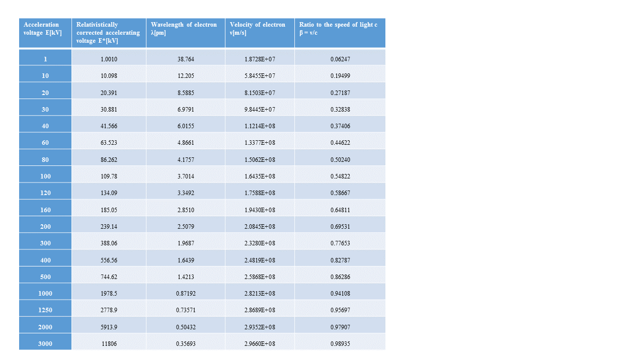
- 76 76. relativistic correction
- 77 77. stopping power
- 78 78. large-angle convergent-beam electron diffraction (LACBED)
- 79 79. Dynamic TEM (DTEM)
- 80 80. multiple scattering
- 81 81. escape depth
- 82 82. many-beam approximation
- 83 83. elastically scattered electron
- 84 84. single particle analysis
- 85 85. Cherenkov radiation
- 86 86. ultra-high voltage electron microscope (UHV-EM)
- 87 87. low energy electron microscope (LEEM)
- 88 88.low-angle annular dark-field scanning transmission electron microscopy (LAADF-STEM)
- 89 89. standing wave
- 90 90. diffuse streak
- 91 91. diffractive imaging
- 92 92. diffractogram tableau
- 93 93. Debye-Scherrer ring
- 94 94. Debye-Waller factor
- 95 95. δ fringe
- 96 96. charge and orbital ordering
- 97 97. electron diffraction
- 98 98. electron holography
- 99 99. electron hologram
- 100 100. electron channeling
- 101 101. wavelength of electron
- 102 102. electromagnetic wave
- 103 103. Vortex electron wave
- 104 104. point resolution
- 105 105. equal thickness fringe
- 106 106. projected potential
- 107 107. transmission electron microscope image (TEM image)
- 108 108. penetrating power
- 109 109. transmitted wave
- 110 110. bend contour (equal inclination fringe)
- 111 111. dynamical diffraction
- 112 112. dynamical extinction
- 113 113. Umweganregung
- 114 114. topography
- 115 115. tomography
- 116 116.Thon's curve
- 117 117. nano-beam diffraction
- 118 118. secondary electron
- 119 119. double diffraction
- 120 120. two-beam approximation
- 121 121. thermal diffuse scattering
- 122 122. Howie-Whelan equation
- 123 123. backscattered electron
- 124 124. photo emission electron microscope
- 125 125. optical diffraction method
- 126 126. delocalization
- 127 127. inelastically scattered electron
- 128 128. differential interference contrast
- 129 129. first zero
- 130 130. Fermat's principle
- 131 131. phonon
- 132 132. Fraunhofer diffraction
- 133 133. Bragg reflection
- 134 134. Poendel Loesung
- 135 135. Friedel's law
- 136 136. Brillouin zone
- 137 137. Fresnel diffraction
- 138 138. Bloch wave
- 139 139. Fresnel fringes
- 140 140. dispersion surface
- 141 141. mean free path
- 142 142. mean inner potential
- 143 143. Bethe's method
- 144 144. Poisson distribution
- 145 145. Born approximation
- 146 146. marker method
- 147 147. multislice method
- 148 148. bright-field image
- 149 149. Moire fringe
- 150 150. Young fringe
- 151 151. Finite element method
- 152 152. Laue function
- 153 153. Laue condition
- 154 154. Laue zone
- 155 155. Rutherford scattering
- 156 156. Lichte focus
- 157 157. critical-voltage effect
- 158 158. excitation error
- 159 159. Lorentz electron microscopy
- 160 160. rocking curve
- 161 161. Ronchigram
- 162 162. Larmor rotation
- 163 163. lens action in the magnetic field
- 164 164. differential phase contrast imaging
- 165 165. Line synchronization
- 166 166. Dwell time
- 167 167. Flyback time
- 168 168. ptychography
- 169 169. autoradiography
- 170 170. reliability factor (R-factor)
1. Eikonal
"Eikonal" is defined as the line of constant optical path length of a wave, which is obtained by multiplying the line of constant phase by λ/2π,whereλis the wave length. The constant plane of eikonal S expresses the plane of the same phase of the wave. The gradient of eikonal, ∇S gives the traveling direction of the wave. |∇S | gives the refractive index at the corresponding position. The concept of eikonal, instead of the refractive index, has been applied to describe the local change of the amplitudes of Bloch waves in a distorted crystal.
2. α fringe
"α fringe" means a fringe contrast, which is observed in bright- and dark-field images under a two-beam approximation condition in the case where the upper and lower crystals are shifted to each other (for example, stacking faults) at an interface oblique to the surface of a crystalline specimen. The end fringes, which appear at the intersection between the interface and the upper and lower surfaces, exhibit symmetric contrast in the bright-field and anti-symmetric contrast in the dark-field with respect to the center of the fringe (specimen).
Related term
stacking fault, two-beam approximation, bright-field image, dark-field image, δ fringe
3. dark-field image
An image that is produced by one diffracted wave in a diffraction pattern formed on the back focal plane of the objective lens, using the objective aperture. A location in the image, where the selected diffracted wave takes place, appears bright. The dark-field image, together with the bright-field image, is used for analysis of lattice defect and measurement of specimen thickness.
Related term
Bragg reflection, diffraction contrast, bright-field image, equal thickness fringe, bend contour (equal inclination fringe)
4. anomalous absorption
When an incident electron beam travels a crystalline specimen, two kinds of electron waves are produced due to the dynamical diffraction effect. That is, one electron wave runs on atomic columns and the other electron wave runs between atomic columns. The former electron wave undergoes a larger absorption than the average absorption, whereas the latter electron wave undergoes a smaller absorption than the average absorption. This phenomenon is termed "anomalous absorption." The main cause of the anomalous absorption is thermal diffuse scattering of incident electrons.
Related term
dynamical diffraction, electron channeling, thermal diffuse scattering, TDS
5. anomalous transmission
When a crystalline specimen is thick, the electron wave that undergoes a larger absorption than the average absorption is damped rapidly; however the electron wave that undergoes a smaller absorption than the average absorption is damped slowly or has a greater transmissivity. This phenomenon is termed "anomalous transmission."
Related term
dynamical diffraction
6. phase contrast
6-1.phase contrast
Contrast produced by changes in phases of scattered waves. The HREM image is formed by the phase contrast. When a specimen is very thin, it is approximated that electron waves hardly suffer absorption but change only their phases (weak phase object approximation). If an aberration-free lens is used to cause interference between transmitted and scattered waves, no contrast appears on the ideal image plane. That is, the phase shift of the scattered waves does not cause the intensity variation in the image. The scattered waves undergo a phase shift of π/2 with respect to the transmitted wave. If the phase of the scattered waves is further shifted by π/2 in such a way that the amount of phase shift due to the spherical aberration of the electron lens is adjusted by the amount of defocus, the resultant phase shift of the diffracted waves becomes πwith respect to the transmitted wave. This phase change of the diffracted waves (π) is converted into the change of amplitude (not complex number but real number), producing contrast in the image due to the interference between the transmitted wave and diffracted waves. When an appropriate defocus amount is selected so that the phase of scattered waves is shifted by π/2 over the wavenumber range as wide as possible and the amplitudes of the waves become as large as possible, the structure image is obtained.
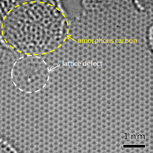
High-resolution TEM image of a single-layer graphene taken at an accelerating voltage of 80 kV.
Since the graphene is regarded as a weak-phase object, the image contrast of the graphene reflects the phase change of electrons scattered by carbon atoms. This image is acquired using an electron microscope equipped with a Cs corrector at a slight defocus to create the phase contrast. Hexagonal grids of the graphene are seen in most parts. In the area enclosed by white dashed lines at the left, a lattice defect is seen. In the area enclosed by yellow dashed lines at the upper left, the graphene is seen to take an amorphous state.
Related term
high-resolution electron microscopy, HREM, weak phase object approximation, crystal structure factor, systematic reflection, Sherzer focus
crystal structure image, lattice image, scattering contrast, diffraction contrast, energy contrast
6-2.differential phase contrast imaging
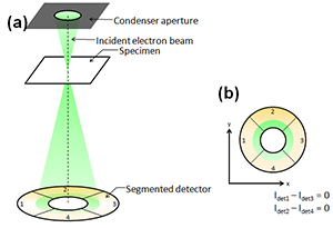
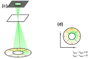
Differential phase contrast imaging is a STEM method to visualize an electromagnetic field in a specimen by measuring the deflection of an electron beam due to the field at each beam-scan point. The beam deflection is measured with a segmented detector or a pixelated detector. When a segmented detector composed of four segments is used (see Figure below), the angle and the direction of the beam deflection (beam shift on the detector plane) are measured from the difference between the signal amounts acquired with the two segments opposed to each other. It is noted that the naming “differential phase contrast” of this imaging method is originated from that the deflection of the electron beam causes the differential or gradient of the phase of the electron wave. Differential phase contrast imaging is utilized for observations of micrometer to nanometer scale magnetic domains. In recent years, this imaging method has been applied to analysis of electric fields, and the electric field at the atomic scale has been observed using a transmission electron microscope equipped with a Cs corrector.
Schematics of a segmented detector
Fig.(a) Schematic of detection of the electron beam deflection in a specimen using a segmented detector (In case that the electron beam is not deflected by the specimen). Fig.(b) A STEM detector in this case is composed of four segments. The shadow of the condenser aperture is projected onto the detector. Top view of the detector and the electron beam seen along the incident beam direction. The signal amounts are the same for the four segments. Thus, there is no difference between the signal amounts acquired from the two segments opposed to each other.
Fig.(c) Schematic of detection of the electron beam deflection in a specimen using a segmented detector (In case that the electron beam is deflected by a specimen). Fig.(d) Top view of the detector and the electron beam seen along the incident beam direction. When the beam is deflected in the positive direction of the x axis, the signal amounts obtained by subtracting Idet3 from Idet1 becomes a negative value, whereas there is no difference between the signal amounts Ide2 and Idet4. As a result, the beam is found to be deflected in the positive direction of the x axis, and the deflection angle is measured from the absolute value of the signal difference.
6-3.Zernike phase contrast
In TEM, "Zernike phase contrast" means contrast which is obtained by converting the phase change of electron waves scattered by a specimen into the amplitude change. The conversion is performed by using a phase plate or a combined effect of the spherical aberration of the electron lens and defocus.
Related term
phase plate, phase contrast
6-4.phase-contrast transfer function (PCTF)
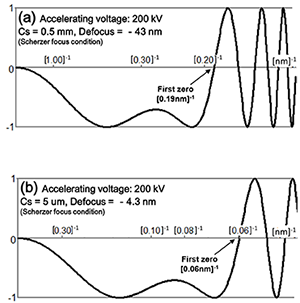
When electrons pass through the objective lens, spherical aberration of the objective lens causes the electron beam to undergo a displacement at the object plane, which is proportional to the cube of the incident angle to the objective lens. For an incident angle, this displacement can be canceled with an opposite displacement proportional to defocus of the objective lens. However, this cancelation is not accomplished for all the incident angles. The cancelation or compensation feature is described by the phase changes of the electron waves passing through the objective lens. That is, the phase changes are given as a function of the incident angle to the lens (or scattering angle from the specimen) and the defocus of the lens for a given Cs coefficient. This function is called “phase-contrast transfer function.”
Example of the phase-contrast transfer function (PCTF) at an accelerating voltage of 200 kV for (a) Cs: 0.5 mm and for (b) Cs: 5 mm. The horizontal axis stands for spatial frequency and the vertical axis for the amount of information on the crystal structure of a specimen transferred to a TEM image. The negative region of PCTF contributes to form dark image for the atom sites and the positive region contributes to form bright image. It is noted that only the image of a very thin specimen, to which the weak phase object approximation can be applied, is interpreted using PCTF.
It is desirable that the value of PCTF is constant (ideally –1 (or +1)) for all spatial frequencies. However, the real TEM accompanies aberrations such as spherical aberration, thus the absolute value of PCTF becomes less than 1 and is not constant. In particular at the high-frequency side, the value fluctuates greatly over the positive and negative values. The structural information on a specimen is transferred without contrast reversal till the frequency at which PCTF firstly crosses the horizontal axis (called First Zero). That is, the inverse of the frequency at First Zero means the resolution of the structural image. When PCTFs (a) without Cs correction and (b) with Cs correction are compared, it is clearly seen that the negative region of PCTF extends to a higher spatial frequency in (b). This indicates that the structural information on a specimen is much better transferred in the case of (b) with Cs correction.
Related term
phase contrast, defocus, first zero
7. single scattering
When the incident electrons that pass through a specimen are scattered only one time until these electrons exit from the specimen, this scattering phenomenon is termed "single scattering."
Related term
multiple scattering
8. interband transition
8-1. interband transition
When the Bragg reflection is treated by the dynamical theory, dispersion surfaces (equi-energy surface), which give allowable wave numbers (equivalent energy planes) near Bragg reflections, are produced. Two dispersion surfaces are produced for each reflection. When the incidence direction of the electron beam onto a specimen crystal (the excitation error of the Bragg reflection) and the surface normal of the specimen are given, the allowed points on the dispersion surfaces are determined. As a result, the wave numbers and amplitudes of the allowed waves in the crystal are determined. If the crystal is perfect, these quantities are kept unchanged. If a defect, for example a stacking fault exists in the crystal, redistribution of the amplitudes occurs on the dispersion surfaces. Wave transfer to a different dispersion surface is called "interband transition." On the other hand, wave transfer within the same dispersion surface is called "intraband transition." The above interband transition in the case of a stacking fault takes place in the scope of elastic scattering. In the case of inelastic scattering, we can consider similar dispersion surfaces which are a little different in their energy from those of elastic scattering. Interband transition occurs at small-angle scattering of thermal diffuse scattering, but intraband transition occurs for plasmon scattering. In the case of core excitation, if interaction that gives rise to the core excitation is small (normally, small), intraband transition occurs. The electrons suffered by the intraband transition produce a similar image to the original image (without transition). However, since the symmetry of the Bloch wave of a dispersion surface is different from that of the other surface, the electrons suffered by interband transition do not form a similar image to the original image. (This term is different from "interband transition" used in solid state physics. In the case of the interband transition in solid state physics, the energy of the electron changes but it does not change in electron diffraction.)
Related term
interband transition, dynamical diffraction, dispersion surface, inelastically scattered electron
8-2. interband transition
A phenomenon in which electrons in a crystal make transitions from the valence band to the conduction band. EELS enables us to obtain the band gap energy from the onset energy of a spectrum that reflects interband transitions.
Related term
valence-loss spectrum (low-loss spectrum)
9. information limit
Information limit indicates the wave number at which phase information carried by the phase-contrast transfer function disappears. That is, it is determined as the wave number at which the envelope function reaches practically zero. The envelope function which gives damping of the phase contrast is determined by an energy spread of the electron beam and stability of the accelerating voltage (these two factors are related to chromatic aberration of the objective lens), stability of the objective lens and the divergence angle of the incident electron beam. The information limit is used as an indication of the resolution of a high resolution image. The resolution of the structure image is given by "first zero" of the phase-contrast transfer function in the ordinary sense. Phase information between the first zero and the information limit can be utilized to obtain a higher resolution of the structure image by computer-processing.
Related term
high-resolution electron microscopy, HREM, crystal structure image, first zero, envelope function
10. weak-beam method
The "weak-beam method" is a technique to take a dark-field image of a weakly excited reflection (for example, the 1st order reflection) at the exact Bragg setting of a high-order reflection (for example, the 3rd order reflection) under a systematic reflection condition. The observation of a dislocation by this method enables us to elucidate only a highly strained part of the dislocation with bright contrast against dark background. Thus, the dislocation is more sharply imaged and the dislocation position is more accurately determined. Accurate analysis of a narrowly extended dislocation can be performed.
Related term
dislocation, partial dislocation, stacking fault
11. kinematical diffraction
An electron that passes through a crystalline specimen is reflected (diffracted) by lattice planes satisfying a Bragg condition. The kinematical diffraction approximation assumes that the Bragg reflection occurs only one time in the specimen. In this context, the reflection intensity is proportional to the square of the crystal structure factor of the reflection. This approximation holds only when a specimen is thin enough (<3 nm). As a specimen is thicker, the reflection occurs many times. In this case, the dynamical diffraction theory must be applied to the interpretation of reflection intensities and electron microscope images.
Related term
Bragg reflection, crystal structure factor, dynamical diffraction
12. satellite reflection
A modulation which has a longer period than that of the fundamental lattice takes place in certain crystals. In such cases, weak diffraction spots due to the modulation appear around the fundamental diffraction spots from the basic lattice. The weak diffraction spots are called "satellite reflections."
13. energy contrast
Image contrast produced by differences in loss energies of inelastically scattered electrons. When the absorption-edge energy of a certain element is chosen with the energy-selection slit, mapping of the selected element in the specimen can be performed. In the future, it will be possible to perform electronic state mapping by selecting the excitation energy of a specific electronic states.
Related term
scattering contrast, diffraction contrast, phase contrast
14. Ewald sphere
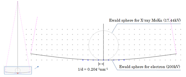
The Ewald sphere is a sphere of the radius defined as the reciprocal of the wavelength of the incident wave 1/λ, and is drawn with the point as the center, the point being at the length 1/λ from a certain reciprocal lattice point along the direction of the incident wave to a specimen crystal. The Ewald sphere explains what Bragg reflections occur using the relation between the incident wave vector and the reciprocal lattice points. All of the reciprocal lattice points on the Ewald sphere satisfy the Bragg condition. For a high energy incident electron (100 or 200 keV), the Ewald sphere can be approximated as a flat plane because the radius of the Ewald sphere is much larger than the distance between the reciprocal lattice points. As a result, the reflections, which appear as cross sections between the Ewald sphere and the reciprocal lattice points, can be indexed easier than the indexing in X-ray diffraction.
The reciprocal lattice points of gold (Au) for [001] incidence (lattice spacing d = 0.204 nm) and the Ewald spheres. The small sphere is the Ewald sphere for X-ray of MoKa (λ = 0.07109 nm) and the large sphere (arc) is the Ewald sphere for an electron beam of 200 kV (λ = 0.002508 nm). The Ewald sphere for the electron beam is displayed up to ±10°, which corresponds to a usual limitation of the acceptance angle of an electron microscope. Blue reciprocal lattice points approximately satisfy the Bragg condition.
Related term
Bragg reflection, reciprocal lattice, reciprocal space, dispersion surface, Laue zone
15. envelope function
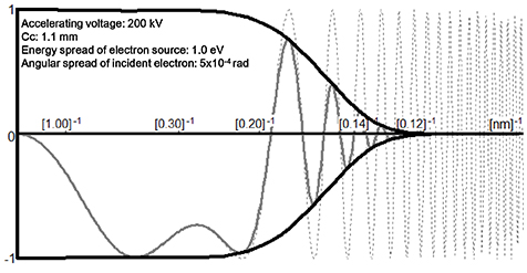
The phase-contrast transfer function plays an important role for the resolution of an HREM image contrast. Another important factor is the envelope function. The phase contrast is damped with increase of scattering angle due to chromatic aberration of the objective lens caused by energy difference in the electron beam, the divergence angle of the electron beam, stability of the objective lens, etc. The function that expresses the damping is called "envelope function." The spatial frequency at which the envelope function becomes practically 0 (zero) is called "information limit."
Example of an envelope function (black line) at an accelerating voltage of 200 kV. The horizontal axis stands for the spatial frequency and the amount of information on the crystal structure of a specimen transferred to a TEM image. The closer the value of the envelope function to 1 (or –1), the more structural information on the specimen contributes to form a TEM image. The closer the envelope function to 0 (zero), the more structural information is lost. The envelope function expresses the degree of coherence of the scattered waves, which is determined by chromatic aberration, angular spread of an incident electron beam, etc. When the chromatic aberration or angular spread is large, the degree of coherence of scattered waves deteriorates quickly with increase of spatial frequency, or the envelope function attenuates quickly to 0. The phase-contrast transfer function (PCTF) should incorporate the effect of the envelope function, then resulting to an actual PCTF as indicated by a gray line. This PCTF shows that the contribution of the scattered waves to the image formation damps with the spatial frequency.
related term
phase-contrast transfer function, PCTF, information limit
16. Auger electron
When an atom at an excitation state makes a transition to the ground state, if its energy is not used to emit characteristic X-rays but used to emit an electron in the atom, the emitted electron is called "Auger electron." The Auger electron energy is characteristic of an element and the escape depth of the Auger electron is very small (0.5 nm to several nm). Thus, the Auger electron is utilized for qualitative and quantitative compositional analysis and electronic structure analysis (analysis of chemical-bonding states) on top surfaces of solids. The accuracy of Auger electron spectroscopy is about 10%.
17. diffracted wave
A wave that undergoes Bragg reflection (diffraction) in a crystalline specimen. In the two-beam dynamical theory, the intensity of the diffracted wave periodically changes with specimen thickness.
Related term
Bragg reflection, transmitted wave, dynamical diffraction, Poendel Loesung
18. interference fringe
A series of light-and-dark fringe that is produced by interference of electron waves.
19. diffraction contrast
Scattered electrons in a crystalline specimen are not continuously distributed with scattering angles but discontinuously distributed as diffracted waves. Diffraction contrast means the intensity change in an electron microscope image that is formed when the diffraction condition is changed with areas of the specimen. In the bright-field image (formed by the transmitted wave), the area where diffraction takes place loses its image intensity, thus getting dark. In the dark-field image (formed by a diffracted wave), the corresponding area gains image intensity, thus getting bright.
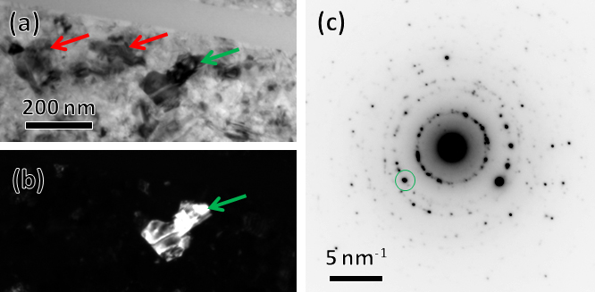
TEM images and a diffraction pattern of polycrystalline Si (a semiconductor interconnect) taken at an accelerating voltage of 200 kV.
(a) Bright-field TEM image. The specimen is composed of many crystalline particles with size of a few 10 nm to a few 100 nm, which exhibit different crystal orientations. In the crystalline particles indicated by red allows and a green arrow, the diffracted waves are intercepted by the objective aperture. As a result, the particles are observed with dark contrast.
(b) Dark-field TEM image taken from the same area in (a). The objective aperture is inserted so that the diffracted wave from the crystalline particles indicated by the green arrow in (a) is acquired. As a result, the particle is observed with bright contrast.
(c) Diffraction pattern. Since the specimen is polycrystalline, the Debye-Scherrer ring is observed. A green circle encloses the diffracted wave from the crystalline particle indicated by the green arrow in (a) and (b).
Related term
scattering contrast, phase contrast, energy contrast, Bragg reflection, bright-field image, dark-field image
20. coherence
"Coherence" is used to indicate the degree of the capability of interference of the electrons emitted from an electron gun. The spatial coherence length of the electrons exiting from the electron source, i.e., the interference distance along the direction perpendicular to the traveling direction of the electrons is determined by the source size and the wavelength of the electrons. A highly coherent electron source is essential for electron holography, where the electron waves are directly brought into interference. Such an electron source or a small-sized source is also required for taking a high-contrast crystal structure image formed. The temporal coherence length, i.e., the interference distance along the traveling direction of the electrons is determined by the monochromaticity and wavelength of the electrons exiting from the source. The temporal coherence has not become a matter of discussion yet in the case of TEM.
Related term
electron holography, envelope function
21. Environmental TEM
The Environmental TEM (ETEM) is a TEM which enables us to observe specimens under a gas-controlled environment. A volume around the specimen is filled with gases so that the pressure of the volume is kept higher than that of the TEM column. The ETEM is classified into two types; isolation-film type and differential pumping type. The former ETEM is equipped with an (gas) environmental cell (EC) in the specimen holder. A passage for gas introduction and evacuation is connected to the EC. There are holes above and below the EC to allow electron-beam transmission. To prevent gas leakage into the microscope column, thin films such as carbon or silicon nitride films (called "insulation films") are sealed to the holes. The latter ETEM is designed to introduce gasses into the specimen chamber in the microscope column. To prevent vacuum deterioration of the column caused by gas diffusion, differential pumping is adopted. For example, multiple orifices are incorporated into the upper and lower parts of the polepieces (on the optical axis). This construction enables differential pumping of spaces isolated by the respective orifices. The ETEM is used for in-situ observation of reaction processes between the specimen and the introduced gasses, observation of water-containing specimens, etc.
Related term
ultra-high voltage electron microscope, UHV-EM
22. interference of electrons
Interference of electrons occurs due to the wave nature of electrons. When the electron waves are superposed, the amplitudes are added when their phases are the same but are canceled when their phases are opposite. When electrons travel a crystalline specimen, they are reflected by various atomic planes in the specimen (Bragg reflections) and diffracted waves are produced in various directions. When these waves meet on the TEM image plane, the waves constructively interfere where their phases are matched, whereas the waves destructively interfere where their phases are opposite. As a result, a fringe or a net image intensity modulation is formed.
Related term
Bragg reflection
23. annular bright-field scanning transmission electron microscopy (ABF-STEM)
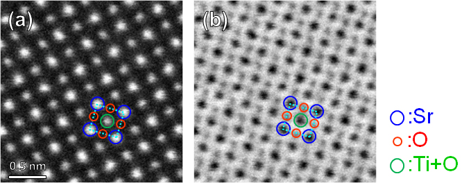
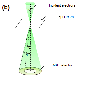
Annular bright-field scanning transmission electron microscopy (ABF-STEM) is a bright-field high-resolution STEM method which preferentially receives only the ring-shaped circumference (e.g. 12 to 24 mrad) of the direct (transmitted)-beam disk using an annular bright-field (ABF) detector, without using the central part of the bright field disk. The integrated intensities of the received electrons are displayed in synchronism with the incident probe position for acquisition of a high-resolution atomic image. The ABF method enables us to effectively visualize atomic columns composed of light atoms. In these light-element atomic columns, the intensities of electrons which travel along the atomic columns parallel to the incident beam, become higher than the scattered electrons due to the electron channeling effect. Thus, the electrons which are incident on the light atomic columns increase to pass through the center hole of the ABF detector. As a result, light elements are effectively imaged as dark spots (image formed by smaller quantity of electrons). On the other hand, the electrons which are incident on the heavy atomic columns increase to scatter at high angles outside of the ABF detector. As a result, heavy atomic columns are also imaged as dark spots. Thus, the ABF method enables us to observe both the atomic columns of relatively heavy elements (transition metals, etc.) and light elements (O, Li, etc.) with the same contrast. HREM and BF-STEM have long been used to visualize atomic columns. However, those two methods necessitate image simulations for correct image interpretation because the intensity of the atomic column largely depends on the defocus amount and specimen thickness. In the ABF-STEM image, (except for extremely thin specimen) the atoms are always imaged as dark spots irrespective of the variation of specimen thickness. Even in the image formed with a certain defocus, atoms are still imaged as dark spots because the incident electrons over a certain angular range reduce the interference effect of each electron. This makes an easy interpretation of the ABF image compared to the HREM and BF-STEM images.
High-resolution STEM images of SrTiO3 taken at the [100] incidence. (Accelerating voltage: 200 kV, Convergence semi-angle of the incident electron beam: 22 mrad) Fig.(a) HAADF-STEM image taken with an acceptance semi-angle of the detector 90 to 170 mrad. Sr columns and Ti + O columns, which are composed of relatively heavy atoms, are clearly visualized. However, the light-atom O columns cannot be observed as bright spots. Fig.(b) ABF-STEM image taken with an acceptance semi-angle of the detector 11 to 22 mrad. The light-atom O columns, which cannot be seen in the HAADF image, are clearly observed as dark spots.
Comparison of Ray diagrams of two detectors
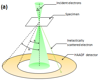
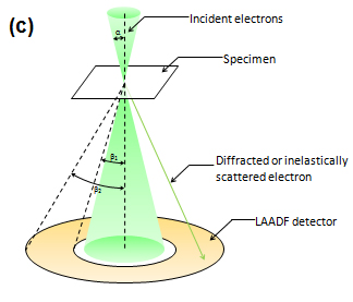
Fig.(a) Relationship between the convergence semi-angle of the incident electron beam and acceptance semi-angles of the detector for HAADF-STEM. Typical inner and outer semi-angles of the detector are respectively β1 = ~50 mrad and β2= ~200 mrad, detecting inelastically scattered electrons at high angles. The value of the convergence semi-angle α is approximately 25 mrad for a 200 kV Cs-corrected TEM. Usually, an ABF detector and a LAADF detector are placed below a HAADF detector.
Fig.(b) Relationship between the convergence semi-angle of the incident electron beam and acceptance semi-angles of the detector for ABF-STEM. The inner and outer acceptance semi-angles of the detector are respectively taken as β1 ≒ α/2 and β2 ≒ α, where a is the convergence semi-angle.It should be noted that the only peripheral part of the bright field disk (without the central part) is used for ABF-STEM. In the case of a 200 kV Cs-corrected TEM, α, β1 and β2 are respectively~25 mrad, ~13 mrad and ~25 mrad.
Related term
high-angle annular dark-field scanning transmission electron microscopy, HAADF-STEM, low-angle annular dark-field scanning transmission electron microscopy, LAADF-STEM, high-resolution electron microscopy, HREM
24. relaxation time
When the external condition of a system changes and then the system reaches its equilibrium state or its steady state under the new condition, the process is called "relaxation." The "relaxation time" means the time that characterizes the velocity of the process from an initial non-equilibrium state to the final equilibrium state.
25. Kikuchi pattern
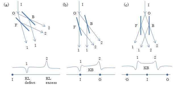
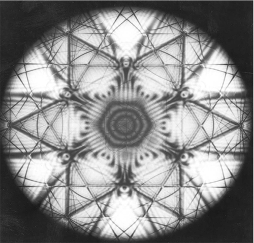
The Kikuchi pattern is a diffraction pattern produced by Bragg reflections of inelastically scattered (thermal diffuse scattering) electrons in a specimen. Since the inelastically scattered electrons distribute over large angles, the Bragg reflections by the inelastically scattered electrons do not form diffraction spots but form a pair of excess and defect lines (Kikuchi lines) respectively by hkl and -h-k-l reflections. The low-intensity (defect) Kikuchi lines appear near side of the direction of the incident beam, whereas the high-intensity (excess) Kikuchi lines appear far side of the direction. When low-order reflections hkl and -h-k-l are strongly excited, a high-intensity (excess) band (Kikuchi band) is formed between the reflections due to a strong dynamical diffraction effect. Kikuchi lines appear sharply for a highly perfect and thick crystal. Kikuchi patterns are effectively used for precise adjustment of a crystal orientation by tilting the crystal for the Kikuchi lines to locate on the Bragg reflection spots.
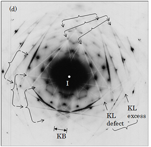
(a) Kikuch lines: When the electrons inelastically scattered at a certain point O in a crystal cause Bragg reflections from the front face (F) and the back face (B) of a crystal plane quite inclined against the direction of incident electrons I, a pair of defect intensity and excess intensity lines which are called Kikuchi lines (KL) are produced at the positions (directions) of the Bragg reflections 1 and 2. The intensity of Kikuchi line (1) near side of I is lower than that of the surrounding area (directions). To the contrary, the intensity of Kikuchi line (2) far side of I is higher than that of the surrounding area (directions). The amplitude of the electrons inelastically scattered at the point O is large at low scattering angles and becomes small as the scattering angle increases. The Bragg reflection (2) from the front face (F) of a crystal plane due to the electrons inelastically scattered near the incident direction I forms strong excess and strong defect Kikuchi lines. The Bragg reflection (1) from the back face (B) of the crystal plane due to the inelastically scattered electrons far from the direction I compensates the contributions from the front face. However, since the compensation by the latter is small, the low intensity (defect) KL (1) is formed near side of I, and the high intensity (excess) KL (2) is formed far side of I. (b) Transformation from Kikuch lines to Kikuchi band: When the inclined angle of the crystal plane becomes small with respect to the direction of the incident electrons I, the difference of the amplitudes of inelastically scattered electrons incident on the reflection planes F and B becomes small. As a result, the bell-shaped intensity of Kikuchi lines becomes low, the symmetrical feature is lost, but an asymmetric (dispersion type) intensity starts to appear. (c) Kikuchi band: When the crystal plane becomes symmetric with respect to the direction of the incident electrons (I), the amplitudes of inelastically scattered electrons become equal for the Bragg reflections 1 and 2. As a result, the bell-shaped intensity vanishes and then, the dispersion type intensity is formed due to a strong dynamical diffraction effect. In the angular region between the positions (directions) 1 and 2, the intensity becomes higher than outside the region. This high intensity band is called Kikuchi band (KB). (d) Kikuchi pattern obtained from a Si single crystal: Many pairs of Kikuchi lines due to high-order reflections are seen. In the vicinity of a symmetric incidence, a Kikuchi band is seen between “G = 220 reflection” and “G = -2-20 reflection”. The low-intensity (defect (dark)) Kikuchi lines appear near side of the incident beam direction, whereas the high-intensity (excess (bright)) Kikuchi lines appear far side of the direction. (However the Kikuchi pattern below is shown with reversal of bright and dark.)
Related term
lattice vibration, thermal diffuse scattering, TDS, inelastically scattered electron, elastically scattered electron, Bragg reflection
26. reciprocal space
A space constructed by reciprocal lattices. In a TEM, the "reciprocal space" appears in the back focal plane of the objective lens on which a diffraction pattern is formed.
Related term
reciprocal lattice, real space
27. reciprocal lattice
"Reciprocal lattice" is a set of points which have distances inversely proportional to the spacings of lattice planes of a real lattice in the directions perpendicular to the original lattice planes. The reciprocal lattice is generated automatically from the real lattice through a mathematical relation.
Related term
real lattice
28. CAT(composition analysis by thickness-fringe)method
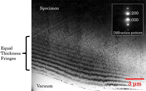
Keyword “CAT(composition analysis by thickness-fringe)method” The "CAT" method is devised to determine the compositions of layer materials that have the same lattice spacing but have different compositions between the layers, like an artificial lattice material of AlxGa1-xAs. Utilizing the fact that the distance between thickness fringes (extinction distance) is inversely proportional to the crystal structure factor, this method determines the compositions of the different layers by measuring the difference of the extinction distances between the layers of a wedge-shaped specimen.
Related term
equal thickness fringe
29. absorption potential
When incident electrons strike constituent atoms in a specimen, the incident electrons undergo inelastic scattering. Inelastically scattered electrons do not interfere constructively with elastically scattered electrons, thus giving rise to absorption or attenuation of elastic scattering. This effect can be taken into account in the elastic scattering theory through imaginary potential or "absorption potential."
Related term
inelastically scattered electron
30. boundary condition
The boundary condition is the condition which should be satisfied by the solution function of the differential equation of a scattering problem at the boundary of a crystal. The boundary conditions in the case of the Bethe' s method for the amplitudes of transmitted and diffracted waves are as follows: 1) The amplitudes of the incident electron wave and those inside the crystal are the same at the entrance surface. 2) The tangential components of those electron waves are the same at the entrance surface.
Related term
Bethe's method
31. forbidden reflection
Even when a set of lattice planes of a crystal satisfies the Bragg condition, its reflection intensity becomes 0 or vanishes if its crystal structure factor is 0 (zero). Such a reflection is called "forbidden reflection." There are two kinds of forbidden reflections, which occur due to the type of space lattice and the symmetry element of the space group.
Related term
extinction rule, Bragg reflection, crystal structure factor, space lattice, crystallographic space group
32. spatial frequency
When considering an electron microscope image as a superposition of electron waves, spatial frequency is expressed as the reciprocal of wavelengths of these waves that are components of the image. The intensity distribution with respect to the spatial frequency is called "power spectrum."
33. accidental reflection
"Accidental reflection(s)" are reflections excited, other than systematic reflections.
Related term
systematic reflection
34. cryo-electron microscopy
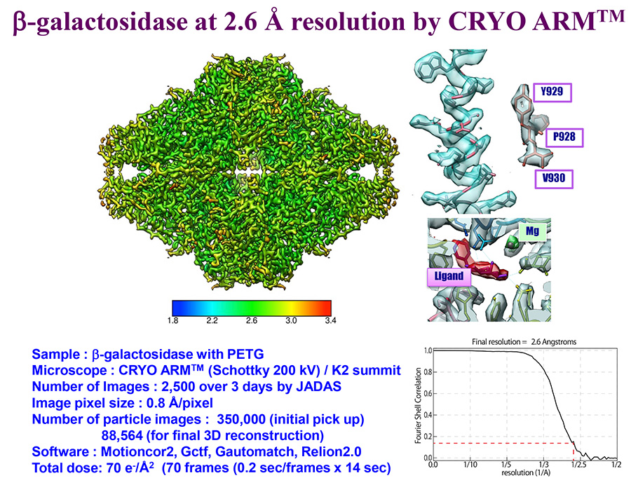
"Cryo-electron microscopy" is a microscopy method used for the observation of biological specimens at the temperature of liquid nitrogen or liquid helium. The biological specimens of purified proteins, viruses, lipid molecules, etc. are prepared by various freezing methods (ice embedding, freeze sectioning, etc.) without staining, and are inserted into a microscope with the specimens kept frozen. Since biological specimens are mostly composed of light elements, scattering contrast is extremely weak to observe. Thus, the specimen is observed using phase contrast produced at a defocus of a few μm.
For inserting the low-temperature (frozen) specimens, two techniques are available: the use of a cryo-transfer holder or a dedicated cryo-electron microscope which has an automatic specimen transfer mechanism.
3D structure analysis methods using cryo-electron microscopy include single particle analysis and tomography.
Related term
ice embedding, freeze sectioning, cryo-transfer holder
35. Green's function
The Green's function, G(r, r'), provides a response at point r from a point scatterer located at r'. The Green's function in the case of the dynamical theory of electron diffraction is (-1/4π)・exp (i k|r - r'|)/|r - r'|.
36. systematic reflection
A series of reflections g, 2g, 3g... aligned in a certain direction (for example, 100, 200, 300...) in an electron diffraction pattern. Reflections other than "systematic reflection(s)" are called "accidental reflection(s)."
Related term
accidental reflection
37. crystal structure factor
The crystal structure factor gives the amplitude and phase of a diffracted wave from a crystal. The factor is determined by the atom species and their positions in a unit cell.
Related term
atom form factor
38. crystal structure analysis
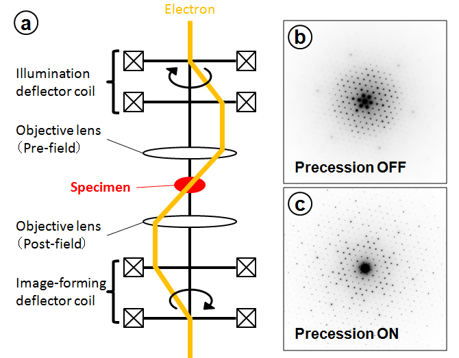
For crystal structure analysis, the electron microscope (TEM) image is not used, but the electron diffraction is used because the spatial resolution of the TEM is around 0.1 nm, but the electron diffraction pattern achieves a spatial resolution of 0.001 nm. In structure analysis, there are two methods; one is to use kinematical diffraction, the other is to use dynamical diffraction. The former is applied when a crystalline specimen is thin and consists of light elements and the dynamical diffraction effect can be neglected. Actually, this method is used for protein crystal analysis. The intensities of each reflection are measured from a diffraction pattern. The phases of the reflections are obtained from the real and imaginary parts of the scattering factors which are obtained by Fourier transform of the corresponding TEM image. Then, the structure is obtained by Fourier synthesis of the intensities and phases. The latter method, which uses convergent-beam electron diffraction (CBED), is applied to structure analysis of nano-scale crystals in the field of materials science. The CBED method has more advantage to study the secondary structure of solid materials, or local structures due to lattice defects and lattice strain than to study the primary structure of crystals. A disk diffraction pattern is acquired by illumination of an electron beam with an incidence angle of several 10 mrad on a small specimen area of a diameter of 10 nm or less. The acquired disk diffraction pattern (CBED pattern) exhibits a two-dimensional rocking curve (intensity distribution) corresponding to the spread of the incidence beam angle. (The CBED pattern appears to be complex due to the dynamical diffraction effect, thus the pattern is greatly different from the Laue function or the rocking curve which is expected from kinematical diffraction.) The crystal structure is solved by the fitting between the simulated CBED pattern obtained by the full dynamical calculation and the experimentally-acquired CBED pattern. Since the phases of the diffracted waves are reflected in the diffraction intensities due to multiple diffraction effects, separate determination of the phases of the diffracted waves is not necessary, which is needed in the case of kinematical diffraction. In addition, an energy filter is effectively used to remove inelastic scattering. The third method is the pre-session method. In this method, to avoid the strong dynamical diffraction effect using illumination of a cone-shaped incident beam on a crystalline specimen with a tilt angle of several degrees from a zone axis, the intensities produced by the cone illumination are added for each reflection. The crystal structure is solved by applying the kinematical theory using the obtained intensities, where the direct method for X-ray diffraction is used to estimate the phases of the diffracted waves.
Related term
crystal structure, electron diffraction, kinematical diffraction, dynamical diffraction, convergent-beam electron diffraction, CBED, rocking curve, Laue function, energy filter
39. crystal structure image
HREM, which allows wave interference between transmitted and diffracted waves to be caused, enables us to obtain an image exhibiting the crystal structure of a thin crystalline specimen (thickness <10 nm). This image is obtained at the defocus condition, which is determined by the spherical aberration of the objective lens and the accelerating voltage of the incident beam (Scherzer focus). The image is taken by setting the electron beam parallel to a low-order zone axis and by passing a transmitted beam and many diffracted beams through the objective aperture. When the image is not taken at Scherzer focus, it is called "lattice image," which does not always correspond to the crystal structure. Three important factors to take an image corresponding to the crystal structure are: (1) Preparation of a sufficiently thin crystalline specimen, (2) High-accuracy adjustment of the crystal orientation, and (3) Adjustment of the Scherzer focus condition.
Related term
high-resolution electron microscopy, HREM, phase contrast, Sherzer focus, zone axis, lattice image
40. atom form factor
A scattering amplitude of an incident electron generated by an atom. The scattering angle dependence on the scattering amplitude is given by the form of the atom. Incident electrons are scattered by the electrostatic potential that is created by an atomic nucleus and surrounding electrons. (X-rays are scattered by electrons). The atom form factor is used to calculate the crystal structure factor.
Related term
crystal structure factor
41. damping
In wave propagation, "damping" means that the amplitude of a wave is decreasing as the wave is traveling.
42. optical potential
A potential to which the imaginary part is added to incorporate the effect of absorption of an incident beam in a specimen. In the explanation of a TEM image using the dynamical theory, the optical potential is used. The absorption effect which gives the imaginary part of the potential includes plasmon excitation, thermal diffuse scattering and single-electron excitation. Plasmon excitation contributes to the average (normal) absorption and thermal diffuse scattering to the anomalous absorption. Single-electron excitation gives little effect to the anomalous absorption comparing to thermal diffuse scattering.
43. high-angle annular dark-field scanning transmission electron microscopy (HAADF-STEM)
High-angle annular dark-field scanning transmission electron microscopy (HAADF-STEM) is a STEM method which receives inelastically scattered electrons or thermal diffuse scattering (TDS) at high angles using an annular dark-field (ADF) detector (~50 to sufficiently high angle; e.g. ~200 mrad). A STEM image is acquired by displaying the integrated intensities of the electrons in synchronism with the incident probe position. As the HAADF image intensity is reported to be proportional to 1.4 square to a square of the atomic number, heavy atoms are observed brighter, but light atoms are difficult to be observed. The HAADF image is easily interpreted due mainly to two reasons. 1) No multiple scattering arises because the scattering cross section of TDS at high angles used for the imaging is small. 2) The interference effect of electrons does not take place for the imaging (non-interference image). The resolution of the HAADF image is almost determined by the incident probe diameter on the specimen. A high-performance STEM instrument provides a resolution better than 0.05 nm. A combined use with EELS, which uses electrons transmitted through the center hole of the ADF detector, enables element analysis column by column. Nowadays, the annular bright-field (ABF) STEM and the low-angle annular dark-field (LAADF) STEM are utilized as STEM methods to effectively visualize light atoms.
Fig.(a) Relationship between the convergence semi-angle of the incident electron beam and acceptance semi-angles of the detector for HAADF-STEM. Typical inner and outer semi-angles of the detector are respectively β1 = ~50 mrad and β2 = ~200 mrad, detecting inelastically scattered electrons at high angles. The value of the convergence semi-angle α is approximately 25 mrad for a 200 kV Cs-corrected TEM. Usually, an ABF detector and a LAADF detector are placed below a HAADF detector.
Related term
scanning transmission electron microscope (STEM) image, annular bright-field scanning transmission electron microscopy, ABF-STEM, low-angle annular dark-field scanning transmission electron microscopy, LAADF-STEM, high-resolution electron microscopy, HREM
44. lattice fringe
The lattice fringe is a periodic fringe in a TEM image, which is formed by two waves; a transmitted wave exiting from a crystal and a diffracted wave from one lattice plane of the crystal. The spacing of the fringe corresponds to that of this lattice plane.
Related term
lattice plane
45.lattice vibration
Constituent atoms in a crystal vibrate around their equilibrium positions due to thermal energy. "Lattice vibration" means that atoms vibrate each other with a specific phase relationship. When the incident electrons on a specimen are scattered with the exciting lattice vibrations, a diffuse intensity distribution is created. This scattering is called thermal diffuse scattering.
Related term
thermal diffuse scattering, TDS, phonon
46. lattice image
HREM, which allows wave interference between transmitted and diffracted waves to be caused, enables us to obtain a lattice image of a thin crystalline specimen at an appropriate defocus of the objective lens. The lattice image (intensity distribution) does not always correspond to the electrostatic potential in the crystalline specimen projected along the direction of the incident electron beam (projected potential). However, the lattice image displays correctly the periodicity of a crystal. When the image is obtained at the defocus condition, which is determined by the spherical aberration of the objective lens and the accelerating voltage of the incident beam (Scherzer focus), it corresponds fairly well to the electrostatic potential (atomic arrangement) in the crystal. This image is called "crystal structure image."
Related term
high-resolution electron microscopy, HREM, phase contrast, Sherzer focus, crystal structure image
47. higher-order Laue zone (HOLZ) reflection
"Laue zones" are defined as the reciprocal lattice planes perpendicular to the direction of the incident beam. A Laue zone containing the point of origin (reciprocal lattice point corresponding to the incidence point) is called the zeroth-order Laue zone (ZOLZ). The Laue zone of the n-th-order counted from the point of origin in the opposite direction of the incident beam is called the n-th-order Laue zone. Laue zones other than ZOLZ are termed "higher-order Laue zones (HOLZ)." The HOLZ reflections appear as narrow ring lines at positions distant from the center of a CBED pattern. The HOLZ reflections provide three-dimensional information on a crystal, whereas, the ZOLZ reflection gives only two-dimensional information on a crystal. The HOLZ reflections have larger diffraction vectors and their positions are sensitive to a slight change of the lattice parameters. Thus, these reflections are efficiently used for high-accuracy analysis of lattice distortions and crystal structures.
Related term
convergent-beam electron diffraction, CBED, Laue zone, zeroth-order Laue zone (ZOLZ) reflection
48. high-resolution electron microscopy
A technique of transmission electron microscopy to obtain a lattice image or a crystal structure image from a thin specimen by utilizing wave interference between transmitted and diffracted waves using a TEM equipped with a small Cs objective lens. An image which corresponds to the crystal structure is obtained by precisely adjusting the incident beam orientation to a zone axis and by setting the focus of the objective lens to Scherzer focus. The spatial resolution depends on the Cs value of the objective lens and the accelerating voltage of the incident beam. When the specimen is thick (more than 10 nm), the image obtained does not well correspond to the crystal structure due to the dynamical diffraction effect. A combined use with a HAADF-STEM image enhances the reliability of the image interpretation. HREM is used for analysis of crystal structures and lattice detects, including interface structures.
Related term
phase contrast, crystal structure image, lattice image, dynamical diffraction, high-angle annular dark-field scanning transmission electron microscopy, HAADF-STEM, spherical aberration, zone axis
49. electron backscatter diffraction
A Kikuchi pattern, which is produced by inelastically backscattered electrons emitted from a specimen, sensitively changes with specimen orientation. "Electron backscatter diffraction (EBSD)" is a method for obtaining crystal-orientation distribution images of crystal grains of a polycrystalline specimen. To obtain the image, the incident electron beam (probe) is scanned over the specimen surface, and the orientation change of the Kikuchi pattern is observed. EBSD provides an image with a spatial resolution of ~0.1 μm and an angular resolution of ~1°. The angular range acquired by EBSD is ~20°. Normally, EBSD is performed in a SEM though this may be performed also in a TEM.
Related term
Kikuchi pattern
50. Cornu spiral
"Cornu spiral" is a graphical presentation of the diffraction amplitude produced by Fresnel diffraction (Fresnel integral) on the complex plane (Gaussian plane) with the integration range (length from the source to the observation point) as a variable, resulting in a spiral shape. The diffraction intensity obtained by Fresnel diffraction is calculated as the square of the length of the line drawn from the start point (corresponding to the position of the source) to the end point (the observation point) of the Cornu spiral.
Related term
Fresnel diffraction, amplitude-phase diagram
51. Five Seidel aberrations
Aberrations are departures of the path of electron beams from the path of the ideal (Gaussian or paraxial) imaging. The term, "(five) Seidel aberrations," is the generic name of the third-order aberrations (third order with respect to the product of α (angle between the electron beam and optical axis) and r (distance of the electron beam from the optical axis)), which occurs for a monochromatic but non-paraxial electron beam. The five aberrations are (1) spherical aberration (proportional to α3), (2) (off-axial) coma aberration (proportional to rα2), (3) off-axial astigmatism (proportional to r2α), (4) curvature of image field (proportional to r2α), and (5) distortion (proportional to r3). In the case of an electron microscope, since the specimen area magnified by the objective lens, the first-stage lens, is very small (r ~0), it is enough to consider the beams passing through the optical axis. Thus, the spherical aberration is most important for the objective lens. The (off-axial) coma aberration is next most important theoretically. Although an example of coma correction has been reported, the effect of coma aberration is small for high magnification images. Since the magnified images or the objects for the intermediate and projector lenses are not small, the aberrations produced by the beams passing through the positions distant from the optical axis give definite contributions. That is, off-axial astigmatism, curvature of image field and distortion are more important for the lenses at successive stages. In recent years, the spherical aberration has been successfully corrected.
Related term
spherical aberration, fifth-order spherical aberration, (off-axial) coma aberration, off-axial astigmatism and curvature of image field
distortion, 5th order aberrations, Cs corrector, geometrical aberration, wave aberration, combination aberration
52. reference wave
In electron holography, the "reference wave" is an electron wave directly coming from the electron source, which interferes with the transmitted wave suffered by a phase shift through an object. The two waves are superposed by an electron bi-prism to obtain an electron hologram.
Related term
electron holography, electron hologram, electron biprism
53. scattering angle
"Scattering angle" means the angle of an electron scattered by an atom in a specimen. It decreases with the scattering angle. The scattering amplitude is larger for the atom with a larger atomic number.
Related term
scattering cross section
54. scattering contrast
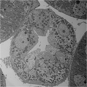
Incident electrons are scattered by constituent atoms in a specimen. When scattered electrons are stopped by the objective aperture, those scattered electrons act as if there arises electron absorption in the specimen. This is expressed as scattering absorption. The scattering cross section of the electron becomes larger as the mass of the atom is larger, and then image contrast produced by differences in scattering amount is termed “scattering contrast.” Since the scattering cross section for electrons is large for the atom with a large mass, the scattering contrast is sometimes called “mass contrast.” The contrast of a TEM image taken from a non-crystalline specimen is explained by the scattering contrast. In the case of a crystalline specimen, elastically scattered waves behave as diffracted waves. Thus, this image contrast is interpreted by the behavior of the diffracted waves.
TEM image of kidney tubules of a mouse taken at an accelerating voltage of 120 kV.
The specimen was chemically fixed using gultaraldehyde and osmium tetroxide and then, subjected to electron staining by uranium acetate and lead citrate. The parts containing heavy elements (osmium, uranium and lead) scatter more electrons at large angles (than the areas containing light elements), and such electrons are intercepted by the objective aperture. As a result, the parts are observed with low intensity (as dark).
Related term
diffraction contrast, phase contrast, energy contrast, electron staining, negative staining, en bloc staining, shadowing
55. scattering cross section
"Scattering cross section" is a probability of scattering of an electron by an atom, expressed by unit of area. It is large at low scattering angles and becomes small at high scattering angles because the atom has a finite size.
56. Scherzer focus
When a high resolution structure image of a phase object is taken in the TEM mode, "Scherzer focus" is used as the defocus condition, which is determined by the spherical aberration of the objective lens so that the phase of diffracted waves is shifted by 1/4 wavelength (or a phase of π/2) of the electron wave over a wide range of spatial frequencies.
Related term
phase contrast, crystal structure image, spatial frequency, first zero, Lichte focus
57. weak phase object approximation
An approximation that is used for interpreting an HREM image. A specimen is regarded as an object that does not change the amplitude of the incident electron wave but slightly changes the phase of the wave. This approximation holds well for a very thin specimen composed of light atoms. In this case, a structure image obtained at Scherzer focus exhibits the projected potential of a crystal. When the specimen is thick, image interpretation is necessary by applying dynamical diffraction that takes account of multiple scattering.
Related term
phase contrast, high-resolution electron microscopy, HREM, Sherzer focus, crystal structure image, projected potential, multiple scattering,
dynamical diffraction
58. convergent-beam electron diffraction
58-1. convergent-beam electron diffraction(CBED)
A method for qualitative and quantitative analysis of crystal structures from a disk diffraction pattern, acquired by illumination of a cone-shaped convergent electron beam on a small specimen area with a diameter of 10 nm or less. The CBED disk displays the intensity distribution corresponding to changes of diffraction conditions (rocking curve). The method enables us to determine not only specimen thickness, lattice parameter, crystal symmetry (point group and space group) and characteristics of a lattice defect, but also a crystal structure (refinement of atomic coordinates, Debye-Waller factors, low-order structure factors (potential distribution)). When the large-angle convergent-beam electron diffraction (LACBED) technique is applied, the characteristic feature of a lattice defect is easily and unambiguously identified and the strains (and a dislocation) at interfaces of a multi-layer material are determined with a high accuracy. The use of an energy filter allows us to conduct more accurate structure analysis.
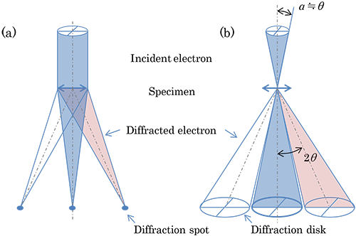
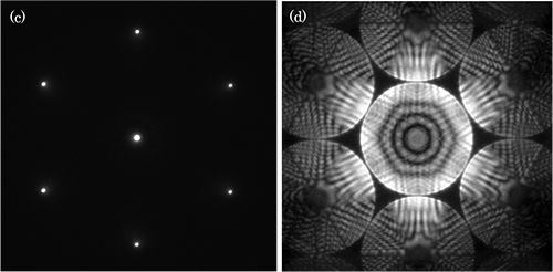
(a) Conventional electron diffraction (Selected-area diffraction) Illuminating a parallel electron beam onto a specimen forms a spot diffraction pattern on the back focal plane of the objective lens. This diffraction pattern is magnified with the imaging lens system and then displayed on a screen. In the figure, the ray path with the imaging lens system is omitted.
(b) Convergent-beam electron diffraction Illuminating a cone-shaped electron beam onto a specimen forms a disk diffraction pattern on the back focal plane of the objective lens. This diffraction pattern is magnified with the imaging lens system and then displayed on a screen. In conventional CBED, the convergence semi-angle a is limited at the maximum to the Bragg angle q to avoid the overlap of adjacent diffraction disks.
(c) Example of Conventional electron diffraction (Selected-area diffraction) pattern. Diffraction pattern of Si [111] taken at an accelerating voltage of 200 kV.
(d) Example of Convergent-beam electron diffraction pattern. CBED pattern of Si [111] taken at an accelerating voltage of 200 kV by eliminating energy loss electrons (Zero-loss pattern).
Related term
electron diffraction, crystal structure, lattice parameter (constant), crystallographic point group, crystallographic space group, lattice defect, large-angle convergent-beam electron diffraction, LACBED, energy filter
58-2. large-angle convergent-beam electron diffraction
In ordinary CBED, if the angular diameter of a diffraction disk exceeds the Bragg angle, the disk overlaps with an adjacent diffraction disk. Thus, the angular diameter is limited to an angle smaller than the Bragg angle. The use of the "large-angle convergent-beam electron diffraction (LACBED)" technique breaks through the angular limitation. Using a condenser-objective (C-O) lens, when a specimen is placed on the focus position of the C-O lens, the bright-field and dark-field images are formed on the image plane (on the selector aperture) but these images are superposed with each other. When the specimen is shifted upper or lower from the focused position of the incident beam, the bright-field and dark-field images on the selector aperture are separated. If only the bright-field image is chosen with the selector aperture and the intermediate lens is set to take a diffraction pattern (the diffraction mode), the bright-field diffraction disk covers an angle of three to four times larger than that for the ordinary CBED disk. Since the LACBED pattern contains information on both the image and diffraction pattern, it is effectively utilized for identification of lattice defects and analysis of strains at interfaces.
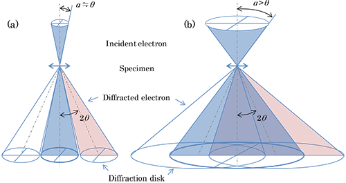
(a) In the case of convergence semi-angle to be equal to the Bragg angle or smaller. In conventional CBED, the convergence semi-angle a is limited at the maximum to the Bragg angle θ to avoid the overlap of adjacent diffraction disks.
(b) In the case of the convergence semi-angle to be larger than the Bragg angle. When the convergence semi-angle a exceeds the Bragg angle θ, the adjacent diffraction disks overlap, thus making it impossible to extract information on each diffraction disk.
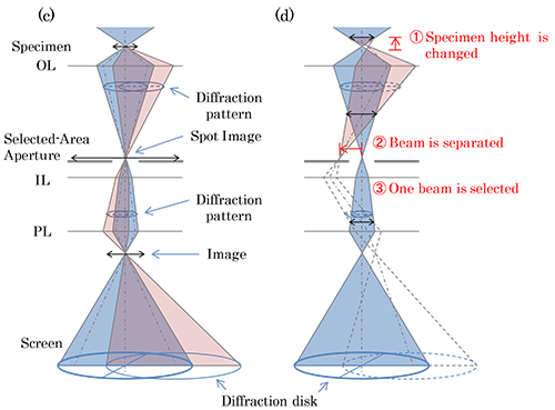
(c) Ray diagram of conventional CBED where the convergence semi-angle is set to an angle larger than the Bragg angle. In conventional CBED, the incident beam is focused on a specimen and the objective lens is focused on the specimen. A diffraction pattern is formed on the back focal plane of the objective lens and an image of the specimen (a spot image in this case) is formed on the selected-area aperture. When the convergence semi-angle of the incident electron beam is set to an angle larger than the Bragg angle, a transmitted wave disk and diffracted wave disks overlap with each other on the back focal plane of the objective lens. The image formed by the transmitted wave and images formed by diffracted waves are superposed on the selected-area aperture to form a spot image.
(d) Ray diagram of LACBED. ①In LACBED, the specimen position is shifted to a higher (lower) position from the focused position of the incident beam without changing the excitation of the objective lens. ②The diffraction pattern is formed on the back focal plane of the objective lens as it is in (c). The image of the specimen, which is formed on the selected-area aperture in (c), is shifted to an upper (lower) position, and on the selected-area aperture the (spot) image of the transmitted wave and (spot) images of the diffracted waves are separated. ③If only the transmitted spot (beam) is selected using the selected-area aperture in the image observation mode of the intermediate lens system, and then the intermediate lens system is switched to the diffraction mode, a large-angle convergent-beam electron diffraction (LACBED) pattern formed only by the transmitted wave is obtained. The LACBED pattern removes the overlap due to the diffracted wave disks and extends its angular diameter beyond the limitation of the diffraction (Bragg) angle.
LACBED pattern of Si [111] taken at an accelerating voltage of 200 kV.
59. extinction distance
When electrons pass through a crystalline specimen and cause one Bragg reflection to occur (two-beam approximation), if an incident wave reaches a certain depth (t), its amplitude becomes 0 (zero) and the reflected wave becomes maximum. Furthermore, if the incident wave reaches a depth (2t) twice as deep as the previous depth, the amplitude of the reflected wave becomes 0 again and the amplitude of the incident wave becomes maximum. Thus, the amplitudes of the incident and reflected waves exhibit beats with the depth. The distance of one periodicity of the beats is called "extinction distance." The extinction distance is inversely proportional to the crystal structure factor of the operating reflection and the wavelength of the incident electron beam.
Related term
Bragg reflection, two-beam approximation, dynamical diffraction, crystal structure factor, equal thickness fringe
60. defocus
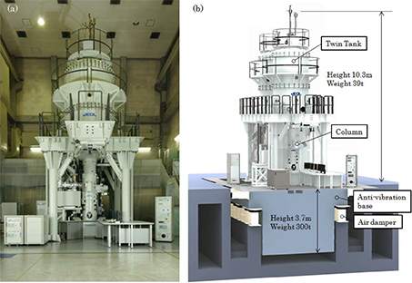
In TEM image observation, the focus of the objective lens is shifted for observing Fresnel fringes or for taking a lattice image or a structure image. This focus shift is called "defocus."
Related term
Fresnel diffraction, lattice image, crystal structure image
61. extinction rule
A rule expressing in what case forbidden reflections occur is termed the "extinction rule." (Forbidden reflection means the extinction of reflections due to scattering factor being 0 (zero) even when the Bragg condition is satisfied.) The extinction of the reflections occurs due to the type of space lattice and due to the symmetry element of the space group. In the former case, reflections vanish even in both the kinematical diffraction case and the dynamical diffraction case. In the latter case, i.e. due to glide planes or screw axes (symmetry elements of the space group), the extinction of the reflections occurs only when kinematical diffraction applies. When the dynamical diffraction effect occurs, the forbidden reflections can have intensity. However, even when there exists the dynamical diffraction effect, extinction occurs at a part of the reflections under a specific beam incidence condition. The extinction appears as a dark line in kinematically forbidden reflections in a CBED pattern.
Related term
forbidden reflection, kinematical diffraction, dynamical diffraction, space lattice, crystallographic space group, glide plane, screw axis
62. amplitude-phase diagram
In the case of the description of the propagation of a diffracted electron wave, let us plot the value of the wave function in the complex plane with coordinates x0, y0. The length of the line drawn from the origin to the point (x0, y0) expresses the amplitude, and the angle between the line and the horizontal axis expresses the phase of the wave. The diagram is called the "amplitude-phase diagram." When a crystal is divided into many layers in its thickness direction, the amplitude and phase of the diffracted wave in each layer is successively added until the bottom surface. The resultant intensity of the wave at the bottom surface is obtained as the square of the length of the line drawn from the origin to the final point (x, y) at the bottom surface. In 1960s, Hirsch et al., for the first time, revealed the image contrast of dislocations and stacking faults using the amplitude-phase diagram.
Related term
Cornu spiral
63. stereo microscopy
A method that obtains stereoscopic images of a specimen. In "stereo microscopy," two electron micrographs are taken from two specimen orientations which differ in a tilt angle by 5° to 10°, and they are viewed independently with right and left eyes. When a complicated dislocation configuration is viewed, diffraction conditions for the two micrographs should be set very similar to reveal the correct three-dimensional structure.
Related term
tomography
64. spin polarized electron
An electron exhibits "up" state or "down" state corresponding to the quantum numbers ±1/2. Recently, a new electron gun technology using a photocathode made of a strained super lattice semiconductor enables the emission of electrons with a spin polarization of more than 90 % at room temperature. Originally, the electron source was developed for collision experiments in the field of elementary particle physics. However, due to the increase of its brightness, the source has recently been applied to photoelectron surface microscopes and transmission electron microscopes (TEM). Then, surface images and TEM images have been obtained. A TEM equipped with the gun allows us to observe the interaction between the incident electron spin and the spins and magnetic moments of the atoms in a specimen.
65. through-focus method
The "through-focus method" is an imaging method used in observation of lattice images or crystal structure images. It acquires the images through gradual change of the focus so that an optimum image can be obtained.
Related term
defocus
66. selected-area diffraction (SAD)
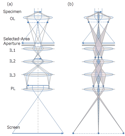
A method for qualitative analysis of crystal structures from a spot diffraction pattern, acquired by illumination of a parallel electron beam on a specimen. By inserting a selector (selected-area) aperture into the image plane of the objective lens, a diffraction pattern is obtained from a specimen area of a several 100 nm diameter. The method enables us to determine the lattice parameters, lattice type and crystallographic orientation of the selected area.
Overview of the standard optical ray diagram of the imaging lens system which is composed of the objective lens (OL) and the four-stage imaging lens system (intermediate lenses (IL1, IL2, IL3) and projector lens (PL)).
(a)Image observation mode, in which the magnified image of a specimen is observed on the screen by focusing the imaging lens to the image formed by the objective lens. In this mode, the selected-area aperture (SA) is inserted into the image plane of the objective lens so that an observation area (field of view) is selected. (b)Diffraction pattern observation mode, in which the diffraction pattern of a specimen is observed on the screen by focusing the imaging lens to the back focal plane of the objective lens. By switching from the imaging mode to the diffraction mode, the diffraction pattern formed only from the selected area in step (a) is obtained.
Related term
electron diffraction, selected-area aperture (intermediate-lens aperture), crystal structure, lattice parameter (constant), crystal orientation
67. electrostatic potential
An electrostatic field is produced by static charge distributions. The electrostatic potential is the potential of the electric field, which is produced by charge distributions. Or the electric field is given by the space derivative of the electrostatic potential. The Fourier transform of the electrostatic potential that is created by the nucleus and orbital electrons of an atom gives the atom form factor.
Related term
atom form factor, projected potential
68. Zernike phase contrast
In TEM, "Zernike phase contrast" means contrast which is obtained by converting the phase change of electron waves scattered by a specimen into the amplitude change. The conversion is performed by using a phase plate or a combined effect of the spherical aberration of the electron lens and defocus.
Related term
phase plate, phase contrast
69. zeroth-order Laue zone (ZOLZ) reflection
"Laue zones" are defined as the reciprocal lattice planes perpendicular to the direction of the incident beam. A Laue zone containing the point of origin (reciprocal lattice point corresponding to the incidence point) is called the "zeroth-order Laue zone (ZOLZ)." The ZOLZ reflections appear around the transmitted beam in a CBED pattern, which have symmetry characteristic of a specimen crystal and show loose angular change. The ZOLZ reflections give two-dimensional information on a crystal projected along the direction of the incident beam.
Related term
convergent-beam electron diffraction, CBED, Laue zone, higher-order Laue zone (HOLZ) reflection
70. fiber pattern
A "fiber pattern" is a diffraction pattern produced from fiber structures in which molecules are oriented regularly only along one axis. The diffraction pattern with the fiber-axis incidence forms Debye-Scherrer rings. As the incidence direction is tilted from the fiber axis, the ring-shaped intensity distributions on the successive Laue zones intersect with the Ewald sphere. A distorted arc diffraction pattern or a fiber pattern appears.
71. transition radiation
When a relativistic charged particle passes from a substance to another with different dielectric permittivities (from vacuum to a substance), electric dipoles are induced on the interface of the substances. At this event, radiation is emitted because the magnitude of the dipole changes with time. This phenomenon is called "transition radiation" and is observed strongly for metals and semiconductors. The emission intensity of the radiation (light) is approximately proportional to the square of the electronic polarizability of the substance.
Related term
Cherenkov radiation, electron energy-loss spectroscopy, EELS
72. correlation method
In three-dimensional tomography, the "correlation method" takes the correlation between each image and performs positional adjustment of these images so that the correlation becomes maximum.
Related term
tomography, marker method
73. scanning low energy electron microscope (SLEEM)
A "SLEEM (scanning low energy electron microscope)" is an instrument to form a surface image, in which the SLEEM image is obtained as follows. An incident electron beam with an energy of several 10 V to several 100 V is used. A small-sized focused electron probe is scanned over the surface of the specimen. Scattered electrons and secondary electrons from the specimen are detected by a SEM detector. To obtain surface information, the specimen area is kept at ultra high vacuum. The SLEEM instrument is usually made by modifying a SEM instrument, thus the beam scan system and secondary electron detector for the SEM instrument are used for the SLEEM instrument. Applying a negative voltage to the specimen gives rise to the formation of a cathode lens or a retarding electric field near the specimen. By varying the value of the negative voltage, the energy of the incident electron beam is varied. A high image resolution is attained at a low incident energy. The present SLEEM achieves a resolution of 10 nm at an incident energy of 10 eV.
Related term
scanning electron microscope, SEM, low energy electron microscope, LEEM
74. scanning electron microscope
74-1. scanning electron microscope (SEM)
An electron microscope in which a small electron probe is scanned over the surface of a bulk specimen, and secondary or backscattered electrons emitted from the surface are collected by a detector, and finally, the intensity of the detected signal is displayed on a computer monitor screen as a series of bright spots synchronized with the scan of the electron probe. An image formed by secondary electrons enables us to observe the fine structure or morphology of the surface of the bulk specimen, whereas an image formed by backscattered electrons provides the difference in the composition of the specimen. The "scanning electron microscope (SEM)" is used by adding various analytical functions (tools) such as EDS and WDS. An important factor that determines the SEM resolution is the size of the incident electron probe (beam) on the specimen. To decrease the probe size, the most essential point is to decrease the size of the electron (emission) source. The cold cathode FEG has the smallest source size, followed by the Schottky FEG, the LaB6 (tip) electron gun, and the tungsten (filament) electron gun. The second most essential point that determines the probe size is the selection of the objective lens. Three types of objective lenses are available; (1) out-lens type, (2) snorkel lens type, and (3) in-lens type. In the out-lens type, a specimen is placed below the objective lens allowing tilting a large specimen. In this lens, limitation on specimen size is not severe but the production of a small beam is difficult because the focal length of the lens becomes large. In the in-lens type, a specimen is inserted into the objective lens in the same manner as the TEM. In this lens, a small probe can be produced because the focal length can be made small. However, the specimen size is limited to several mm. The snorkel lens has a compromise design between the out-lens and in-lens. (The term, "snorkel," originates from the fact that the lens geometry resembles a snorkel used by divers.) A specimen is placed below (not far from) the objective lens. Thus, a relatively small probe can be produced and also a relatively large specimen can be treated. The SEM resolution is degraded at low accelerating voltages due to the chromatic aberration effect. Normally, the resolution is defined at 20 to 30 kV. An ultra-high resolution SEM achieves a resolution of about 1 nm, whereas a general-purpose SEM provides a resolution of about 10 nm. The use of a Cs corrector or a Cc corrector enables a further decrease of the incident-beam size, but causes a disadvantage of a short focal depth because the acceptance angle becomes larger. As the accelerating voltage of the incident electrons is decreased, the penetration depth of the electrons becomes smaller. This reduces a spread of secondary electrons generated by backscattered electrons in the specimen, thus enhancing the image contrast. Advantages of low accelerating voltage include the reduction of the background in the image, the decrease of charging, and the decrease of damage to the specimen. In SEM, charging degrades the image quality. If the current of the incident electrons exceeds the current of electrons flowing out of the specimen, charging takes place. The charging disturbs the image, sometime forming nothing like the true image. When a nonconductive specimen is used, to prevent charging, the specimen is coated with a conductive material, such as noble metal, Al and C. In a low-vacuum SEM, a nonconductive specimen may be observed without coating.
Related term
secondary electron, backscattered electron
74-2. scanning low energy electron microscope
A "SLEEM (scanning low energy electron microscope)" is an instrument to form a surface image, in which the SLEEM image is obtained as follows. An incident electron beam with an energy of several 10 V to several 100 V is used. A small-sized focused electron probe is scanned over the surface of the specimen. Scattered electrons and secondary electrons from the specimen are detected by a SEM detector. To obtain surface information, the specimen area is kept at ultra high vacuum. The SLEEM instrument is usually made by modifying a SEM instrument, thus the beam scan system and secondary electron detector for the SEM instrument are used for the SLEEM instrument. Applying a negative voltage to the specimen gives rise to the formation of a cathode lens or a retarding electric field near the specimen. By varying the value of the negative voltage, the energy of the incident electron beam is varied. A high image resolution is attained at a low incident energy. The present SLEEM achieves a resolution of 10 nm at an incident energy of 10 eV.
Related term
scanning electron microscope, SEM, low energy electron microscope, LEEM
75. scanning transmission electron microscope (STEM) image
"Scanning transmission electron microscope (STEM) image" is obtained as follows. A small-sized, focused electron probe is scanned over a thin specimen using the double-deflection system. The intensity of the transmitted wave (or the diffracted wave) exiting from a point on the specimen is detected with an annular detector. Then, the intensities are displayed on a computer monitor as a series of bright spots in synchronism with the scanning electron-probe. The resolution of the STEM image is determined by the probe diameter. The STEM method has two observation modes; bright-field mode and dark-field mode.
Related term
transmitted wave, diffracted wave, probe diameter, high-angle annular dark-field scanning transmission electron microscopy, HAADF-STEM, annular bright-field scanning transmission electron microscopy, ABF-STEM, low-angle annular dark-field scanning transmission electron microscopy, LAADF-STEM
76. relativistic correction
Relativistic correction is a correction to take in the relativistic effect arising when the velocity of an electron becomes high to an extent which cannot be neglected compared with the velocity of light. In the field of electron microscopy, the relativistic effect due to increase of the mass or decrease of de Broglie wavelength is taken into account by replacing the accelerating voltage with the corrected accelerating voltage. That is, the accelerating voltage after the relativistic correction E* [V] is calculated by the following equation for a given (before relativistic correction) accelerating voltage E [V], here, m0 is the rest mass of an electron, e the elementary charge of an electron, and c the velocity of light.

77. stopping power
"Stopping power" means the average amount of energy loss per unit distance when a charged particle passes through a substance. In the case of TEM, the energy loss occurs mainly due to ionization and excitation of electrons. The "stopping power" is used for calculation of the temperature increase of specimen and the degree of specimen damage.
78. large-angle convergent-beam electron diffraction (LACBED)
In ordinary CBED, if the angular diameter of a diffraction disk exceeds the Bragg angle, the disk overlaps with an adjacent diffraction disk. Thus, the angular diameter is limited to an angle smaller than the Bragg angle. The use of the "large-angle convergent-beam electron diffraction (LACBED)" technique breaks through the angular limitation. Using a condenser-objective (C-O) lens, when a specimen is placed on the focus position of the C-O lens, the bright-field and dark-field images are formed on the image plane (on the selector aperture) but these images are superposed with each other. When the specimen is shifted upper or lower from the focused position of the incident beam, the bright-field and dark-field images on the selector aperture are separated. If only the bright-field image is chosen with the selector aperture and the intermediate lens is set to take a diffraction pattern (the diffraction mode), the bright-field diffraction disk covers an angle of three to four times larger than that for the ordinary CBED disk. Since the LACBED pattern contains information on both the image and diffraction pattern, it is effectively utilized for identification of lattice defects and analysis of strains at interfaces.
Related term
convergent-beam electron diffraction, CBED
79. Dynamic TEM (DTEM)
In an ordinary TEM, the time resolution of image recording is limited to 1/30 seconds (TV rate). However, the Dynamic TEM (DTEM) achieves a much higher time resolution of the order of nano seconds to femto seconds by the combined use of an electron source generating electron pulses and a fast recording system. A DTEM is equipped with a laser-pulse-driven photoelectron source and a pulse-laser specimen-irradiation system. By synchronizing the electron beam pulse with the pulse laser for the specimen, one can observe chemical reaction processes and crystallization processes with such a high time resolution.
80. multiple scattering
When the incident electrons travel a specimen, these electrons strike the constituent atoms in the specimen many times until these electrons exit from the specimen and change their traveling direction. This (scattering) phenomenon is termed "multiple scattering." Among the theories related to multiple scattering, the dynamical diffraction theory, which treats multiple scattering due to elastic scattering (Bragg reflection), provides the intensities of the incident and diffracted waves as a function of specimen thickness and scattering angle.
Related term
dynamical diffraction
81. escape depth
The "escape depth" is the depth of a specimen from which secondary electrons, characteristic X-rays, or Auger electrons can escape.
82. many-beam approximation
Many-beam approximation is an approximation method to interpret the diffraction intensity and TEM image, which takes account of not only a Bragg-reflected beam (diffracted wave) from one lattice plane, but also many reflected beams from other lattice planes.
Related term
two-beam approximation, kinematical diffraction, dynamical diffraction
83. elastically scattered electron
83-1. elastically scattered electron
Elastically scattered electrons are defined as the electrons which are scattered (change in their traveling direction) by constituent atoms in a specimen without losing their energy. When a specimen is a crystal, elastically scattered electrons become diffracted waves that travel in specific directions given by the Bragg condition. As a specimen is thinner, the intensity of a TEM image or a diffraction pattern is explained by elastically scattered electrons. As a specimen is thicker (~10 nm or thicker), the effect of inelastically scattered electrons must be taken into account.
83-2. inelastically scattered electron
Inelastically scattered electrons are defined as the electrons which lose part of their energy (traveling speed becomes slower) through interactions between the electrons and a specimen. The probability of occurring inelastic scattering is small, ~1/10 or less compared with that of elastic scattering. However, as a specimen is thicker (~10 nm or thicker), the inelastically scattered electrons superposed on elastically scattered electrons obscure a TEM image or a diffraction pattern. To remove inelastically scattered electrons, an energy filter is effectively used.
Related term
elastically scattered electron, absorption potential, energy filter, electron energy-loss spectroscopy, EELS, thermal diffuse scattering, TDS
84. single particle analysis
An electron microscopy method to obtain the three-dimensional (3D) structure of biological macromolecules, such as proteins and nucleic acids, by analyzing electron microscope images of the macromolecules (proteins, etc.) recorded as dispersed particles (single particles). A solution containing a protein is made into a thin film on a holey carbon film attached on an EM grid and is then rapidly frozen so that the particles are embedded in an amorphous ice film. TEM images are taken at Liq.N2 temperature, and the 3D structure is reconstructed by image processing and analysis. A number of projection images of the 3D structures of protein particles in various orientations are recorded in the acquired Cryo-TEM images. Each particle image is rotated and translated in the image plane to collect the images having the same external shape and the same density distribution to sort them into groups of different 3D orientations. Then, the images in the same groups are added and averaged to improve the signal-to-noise ratio of the images. Next, the Euler angles of the projection orientations (angles of the particles against the image plane in the present case) are estimated. Finally, the 3D structure of the protein is reconstructed by back projection of these particle images along the estimated Euler angles. Single particle analysis has been dramatically improved in its achievable resolution and practical application by the advent of a CMOS direct electron detector, together with innovations in specimen preparation techniques and analysis software programs. The method is applicable to an extremely small amount of sample solution (protein concentration: several mg/mL, solution volume: several µL/grid), and is especially effective for structural analysis of proteins that are difficult to crystallize. As of 2018, the highest resolution achieved with the method is 0.16 nm.
Specimen preparation and observation method
A highly purified protein solution is prepared in which protein particles with a homogeneous structure are dispersed. The protein particles are ice-embedded by rapid freezing (at –180 °C or less) so as to preserve their structures. It is important that the ice film embedding the protein particles must be prepared as thin as possible to produce high contrast TEM images because proteins are composed of light elements (C, H, O, N, S, etc.) and produce low contrast against the ice film by a small difference between their densities. The specimen grid is inserted into the microscope column with its frozen state kept. TEM images of the specimen are recorded at Liq.N2 temperature. To suppress the damage to the specimen due to electron-beam irradiation, the electron dose onto the specimen must be set low. The specimen is observed using phase contrast because protein particles consisting of light elements are difficult to observe using scattering contrast. For observation of protein particles, a large amount of defocus of the objective lens (–0.5 to several µm) is used to enhance the image contrast, particularly in a low spatial frequency range to allow the detection and orientation determination of the particles.
Image acquisition
Images of protein particles recorded at a low electron dose have a very low-signal-to-noise ratio (S/N). To obtain the particle images with a high S/N, hundreds to thousands of Cryo-TEM images are collected, from which several tens of thousands to several hundreds of thousands of particle images are extracted and added and averaged after image classification and alignment. In recent years, several thousands of Cryo-TEM images are automatically acquired over several days using an automatic image acquisition system. It is emphasized that the electron-beam-induced drift of ice-embedded protein particles is the main cause of degrading the resolution of the TEM image in the single particle analysis method. Extremely high frame rate of direct electron detectors (scintillator not used) that allow single electron counting and movie-mode image recording has improved the resolution of the TEM image. Recording a TEM image in the movie mode at a frame rate of 5 to 10 frames/sec allows the particle image drift to be greatly reduced by post image processing, namely motion correction of the particle images between the frames enables acquisition of high-resolution protein particle images.
Image analysis
From several thousands of the Cryo-TEM images, several tens of thousands to several hundreds of thousands of the protein particle images are automatically extracted using a particle detection software program. Since the particle images are projected in various orientations, the extracted images are rotated and translated so as to sort them out into many classes of the projection images in the same orientations. Then, the images sorted in each class are aligned in their positions and orientations and are averaged. As a result, 100 to 200 protein particle images with a high S/N are obtained. In this step, the 3D orientations of the particle images (Euler angles or the angles of the particles against the image plane in the present case) are not yet determined. To obtain the Euler angles, first an initial particle model with arbitrary orientations is given. Secondary, the projection images of the model are produced. The Euler angle of each particle image is estimated by a comparison of the projection images and the TEM image. The particle TEM images with the estimated Euler angles are subjected to back projection to produce an initial 3D structure of the particle. Then, this 3D structure is subjected to projection again to create the projection images. The re-projected images and the particle TEM images are compared to estimate the Euler angles again. These particle images are back-projected to obtain a better 3D structure in the next step. These steps are repeated until the obtained 3D structure is converged. In each step of calculations, the results are evaluated by statistical approaches. Finally, the most probable 3D structure is obtained.
Comparison with other analytical methods
Structural analysis methods using electron microscopy include Electron Crystallography, Electron Tomography and Single Particle Analysis. In Electron Crystallography, a 2D or thin 3D crystal is prepared and analyzed using techniques similar to those of X-ray Crystallography. Electron Crystallography provides a resolution better than 0.2 nm. In Electron Tomography, one specimen is placed in the specimen holder in the microscope column, and is subjected to serial tilt-series imaging at various angles. Then, back projection is applied to the acquired projection images for obtaining the 3D structure. In the method, it is not possible to improve the signal-to-noise ratio and the resolution of the images by averaging. For biological applications, the method is used for analysis of functional structures at the cell level, its resolution being on the order of several nm to 10 nm. But when the tomogram contains many particles of the same proteins, the use of the sub-tomogram averaging method improves the resolution close to 0.3 nm. Conventionally-used structural analysis methods of proteins are X-ray Crystallography and Nuclear Magnetic Resonance (NMR) spectroscopy. The former method requires a crystal with a size of 10 µm or more. Thus, the method cannot be applied to proteins that are unable to crystallize. The latter method can be used only for proteins with a molecular weight of ~50,000 or less. However, Single Particle Analysis does not have such restrictions and its resolution has been becoming as high as that of X-ray Crystallography, although at present it is still difficult to apply this method to proteins with molecular weight less than 100,000 because of low S/N of their TEM images. In the future, the advancement and the more use of Single Particle Analysis are highly expected. (Proofread by Specially Appointed Professor Keichi Namba and Specially Appointed Associate Professor Takayuki Kato, Osaka University)
Data courtesy: Specially Appointed Professor Keichi Namba and Specially Appointed Associate Professor Takayuki Kato, Osaka University
Related term
tomography
85. Cherenkov radiation
When the velocity of a charged particle exceeds the velocity of light in a substance, light is emitted from the substance. This light is called the Cherenkov radiation. The intensity of the radiation is inversely proportional to the square of the wavelength of the radiation. The Cherenkov radiation is also observed when an electron beam illuminates a specimen in a TEM, which provides information on the refractive index of the specimen.
Related term
transition radiation
86. ultra-high voltage electron microscope (UHV-EM)
"Ultra-high voltage electron microscope (UHV-EM)" is an electron microscope which accelerates electrons with a high voltage of 1000 kV or higher. The wavelength of an electron at 1000 kV is shortened down to 0.00087 nm. Utilizing the short wavelength, a resolution of about 0.1 nm has been obtained, and light elements such as carbons have been clearly observed. However, recent high resolution imaging has been achieved by 300 kV microscopes equipped with a spherical aberration corrector. The advantage of UHV-EM is the capability of observing thick specimens using its high transmission power, of investigating radiation damage of specimens using the high energy electron beam and of investigating chemical reaction at controlled conditions utilizing an enough space of a specimen chamber.
The ultra-high voltage electron microscope (UHV-EM) is an electron microscope which accelerates incident electrons with a high voltage of 1000 kV or higher. The wavelength of an electron at 1000 kV is shortened down to 0.00087 nm. Utilizing the short wavelength, a spatial resolution of the microscope image with about 0.1 nm has been attained. The other advantages of UHV-EM include observation of thick specimens using its high transmission power, investigation of radiation damage of specimens using its high-energy electron beam, and study of chemical reactions under controlled environments by utilizing a large space of the specimen chamber.
related term
point resolution, radiation damage, Environmental TEM
87. low energy electron microscope (LEEM)
A "LEEM (low energy electron microscope)" is an instrument to obtain a surface image of a specimen. The incident electron energy is reduced to several V to several 10 V, and elastically-backscattered electrons from a specimen are accelerated by an electric field just above the specimen. The formed image is enlarged by the imaging lens and observed through a screen or a camera. The spatial resolution of LEEM is 5 to 10 nm. A dark-field image can be obtained by selecting a diffraction spot of LEED (low energy electron diffraction) with an aperture. The specimen area is kept at an ultrahigh vacuum to obtain surface structural information. LEEM is often accompanied with a function of PEEM (photo emission electron microscope) which has the same imaging system as that of LEEM.
Related term
photo emission electron microscope, PEEM
88.low-angle annular dark-field scanning transmission electron microscopy (LAADF-STEM)
Low-angle annular dark-field scanning transmission electron microscopy (LAADF-STEM) is a STEM method which receives diffracted or inelastically scattered electrons at low to medium angles (25 to 60 mrad) using an annular dark-field (ADF) detector. A STEM image is acquired by displaying the integrated intensities of the electrons in synchronism with the incident probe position. It is noted that the LAADF image shows diffraction contrast or difference of specimen thickness dependence. LAADF-STEM is used in place of HAADF-STEM for a specimen composed only of light elements (molecular crystals, two-dimensional crystals, organic materials like macromolecules, biological materials, etc.). This is because the HAADF image does not have a high signal-to-noise ratio due to weak elastic and inelastic scattering at high angles for such light-element specimens. LAADF-STEM enables us to obtain a high-resolution image with a high signal-to-noise ratio whose intensity depends on the atomic number.
STEM images of the cross-sectional thin film of a semiconductor device (an n-channel MOSFET of CPU). (Accelerating voltage: 200 kV, Convergence semi-angle of the incident electron beam: 11 mrad)
Fig.(a) HAADF-STEM image taken at an acceptance semi-angle of the detector of 46 to 208 mrad. As is shown by a blue arrow, only a region where heavy atoms (Ta, W, etc.) exist are observed with bright contrast. Fig.(b) LAADF-STEM image taken at an acceptance semi-angle of the detector of 14 to 63 mrad. SiNx layers in the regions indicated by a red parenthesis are observed brighter than SiO2 regions indicated by a blue parenthesis. Such layer structures are hardly seen in the HAADF image. In addition, the LAADF image also visualizes lattice defects indicated by red allows.
Comparison of Ray diagrams of two detectors
Fig.(a) Relationship between the convergence semi-angle of the incident electron beam and acceptance semi-angles of the detector for HAADF-STEM. Typical inner and outer semi-angles of the detector are respectively β1 = ~50 mrad and β2= ~200 mrad, detecting inelastically scattered electrons at high angles. The value of the convergence semi-angle α is approximately 25 mrad for a 200 kV Cs-corrected TEM. Usually, an ABF detector and a LAADF detector are placed below a HAADF detector.
Fig.(c) Relationship between the convergence semi-angle of the incident electron beam and acceptance semi-angles of the detector for LAADF-STEM. The inner and outer acceptance semi-angles of the detector are respectively taken as that β1 is a little larger than α and β2 is ~60 mrad, where α is the convergence semi-angle. It should be noted that the diffracted waves and inelastically scattered electrons over low to medium angles are used for LAADF-STEM.
Related term
high-angle annular dark-field scanning transmission electron microscopy,HAADF-STEM, annular bright-field scanning transmission electron microscopy, ABF-STEM
89. standing wave
"Standing wave" means that the ratio between the amplitude of a wave at a certain point and that at the other point is constant regardless of time. When an electron wave exactly satisfies a Bragg reflection in a crystal, the incident wave and the diffracted wave form a standing wave.
Related term
Bragg reflection, equal thickness fringe
90. diffuse streak
"Diffuse streak" means the streak intensity appearing in a (selected-area) diffraction pattern. The streak is produced from planar lattice defects (stacking faults, etc.) or linear lattice defects (atomic columns of different species or vacancy columns). Disorder of crystal structures can be deduced from the analysis of the diffuse streak.
91. diffractive imaging
"Diffractive imaging" is a method to reconstruct a structure image of a specimen from a diffraction pattern of the specimen. Since the diffraction pattern is less influenced by lens aberrations, the resolution of the structure image obtained is determined by the maximum diffraction angle of the diffraction pattern, thus a higher-resolution structure image (amplitude image and phase image) than a HREM image (taken by using lenses) can be obtained. This method has actively been studied in the field of X-ray diffractometry, the method being called "Coherent Diffractive Imaging." In electron microscopy, the method is called "Diffractive Imaging" or "Diffractive Microscopy." The method has been applied to carbon nanotubes, etc., and a spatial resolution around 0.1 nm has been obtained. In addition, the method can be applied to not only crystals but also non-periodic structure specimens such as a single-molecule specimen. To reconstruct the image, the Fourier repetitive phase recovery method is used. That is, the magnitudes of the diffraction amplitudes are calculated by the square root of the diffraction intensities taken from a specimen, and random initial phases are given to the diffraction amplitudes. Then, the diffraction amplitudes with the phases are Fourier-transformed to obtain an approximate structure image. The obtained image exhibits structures even in areas exceeding the specimen area from which the diffraction pattern was taken. When the external shape of the specimen is clearly determined, the image intensities from areas except for the external dimension are set to be 0 (zero) (real-space constraint conditions). (On the other hand, when it is difficult to accurately determine the external shape, a specimen area (called "support") that is slightly larger than the external dimension is defined, and the image intensities from areas exceeding the support are set to be 0. Then, the image is inverse-Fourier-transformed to a diffraction pattern. The diffraction amplitudes that do not match the experimental amplitudes are replaced with the experimental values (reciprocal-space constraint conditions), and then Fourier transform is applied again to obtain a structure image. As this procedure is repeated, the true phases of the specimen are gradually recovered and finally, a true structure image of the specimen is obtained. The number of iterations until the recovery of the true phases exceeds several thousands of times. The accuracy of the obtained image is influenced by the parameters such as inelastic scattering contained around the origin of the diffraction pattern, noise from the detection system including its electronic circuits, and the external dimension of the support. It should be noted that when taking the original diffraction pattern, an area of twice the specimen area (support) must be illuminated with an electron beam. This means that the diffraction pattern is sampled with steps twice as small as those corresponding to the original specimen size, enabling us to extract all information contained in the specimen, which is called the over-sampling condition. In an actual experiment, it is needed to create an area where no specimen exists around the specimen and to record a diffraction pattern so as to satisfy the over-sampling condition.
Conceptual diagram of the Fourier repetitive phase recovery method for diffractive imaging. A crystal structure image of a specimen is retrieved from an experimental diffraction data with a good accuracy by applying Fourier transform to the reciprocal space data and then inverse Fourier transform to the obtained real space data repeatedly with giving constraint conditions at each step. To be precise, 1) First, a wave field in the reciprocal space is created by using the diffraction amplitudes obtained from a diffraction pattern and giving random initial phases to the diffraction amplitudes. 2) The wave field formed in the reciprocal space is Fourier-transformed to an image in the real space. 3) The intensities of the image outside the support area are set to be 0 (zero). 4) The corrected image is inverse Fourier-transformed to a wave field in the reciprocal space. 5) The amplitudes of the wave field are replaced to those of the experimental diffraction pattern. Repetition of this cycle enables us to accurately retrieve the phases of diffraction spots in the reciprocal space and the wave field in the real space. 6) Finally, an accurate structure image of the crystalline specimen is reconstructed.
92. diffractogram tableau
"Diffractogram tableau," which is also called "Zemlin tableau," displays two-dimensionally Fourier transform patterns of high-magnification images taken from an amorphous thin film while the azimuthal angle is sequentially changed by a sequential tilt of the incident beam (tilt step: 1 to 2°). Utilizing the degrees of ellipse and symmetries of the patterns, axial astigmatism correction, coma-free axis alignment and three-fold astigmatism correction are executed. When a Rose-Haider-type Cs corrector is installed in a TEM, the use of the diffractogram tableau enables us to correct spherical aberration and four-fold astigmatism and optimize fifth-order spherical aberration. Software that automatically executes these corrections has already been developed.
Figs. (a) and (b) show two diffractogram tableaus without Cs correction and with Cs correction, respectively. The diffractogram tableaus are displayed in the following manner. At the center, a diffractogram obtained without tilt of the incident electron is placed, and around the center, the diffractograms obtained by tilting the incident electron beam are placed according to the tilt angles and azimuth angles. When the incident beam is tilted, the shapes of the diffractograms are distorted depending on the magnitudes and symmetries of the axial (geometrical) aberrations. In Fig. (a), each diffractogram for the tilted electron beam is largely distorted from a perfect circle, which is caused mainly by the third-order spherical aberration. In Fig. (b), the diffractograms taken at the tilted incident beams keep almost circular shape and show small difference between the patterns of the diffractograms, indicating the aberrations being almost corrected.
Related term
Cs corrector, coma-free axis
93. Debye-Scherrer ring
"Debye-Scherrer rings" are concentric diffraction rings produced by Bragg reflections, which are obtained when polycrystalline thin films are illuminated with a highly parallel electron beam.
Related term
Bragg reflection
94. Debye-Waller factor
A factor that expresses an effect of thermal vibrations (lattice vibrations) of atoms. The intensity of Bragg reflections at high angles is damped by the "Debye-Waller factor."
Related term
lattice vibration, Bragg reflection
95. δ fringe
"δ fringe" means a fringe contrast, which is observed in bright- and dark-field images under a two-beam approximation condition in the case where the orientations of the upper and lower crystals are different to each other (for example, twin boundary) at an interface oblique to the surface of a crystalline specimen. The fringe contrast, which appears at two positions (edges) where the interface intersects the upper and lower surfaces, exhibits symmetric contrast in the dark-field and anti-symmetric contrast in the bright-field with respect to the center of the fringe (specimen).
Related term
twins, boundary, two-beam approximation, bright-field image, dark-field image, α fringe
96. charge and orbital ordering
"Charge and orbital ordering" states the charge-ordered state and the orbital-ordered state for 3d electrons in transition metals in a crystal. The charge-ordered state means that two charge states are alternately and regularly arranged. The orbital-ordered state means that orbitals, for example eg orbitals, with one orientation and the other orientation are alternately and regularly arranged. These states emerge in perovskite oxides containing transition metals when composition or temperature is changed. Such super structures in electronic systems are reflected in lattice systems, thus these structures are observed by superlattice reflections in an electron diffraction pattern.
Related term
superlattice
97. electron diffraction
97-1. electron diffraction
A method for obtaining information on crystal structures from diffraction patterns, acquired by electron-beam illumination on a specimen. When a specimen is a crystal, the information on various crystal structures is obtained, which include periodicities, symmetries and ordering of atomic arrangements, and defects of crystal lattices. When a specimen is an amorphous material, the distances between the first, second, ... nearest neighbor atoms and the number of these atoms are obtained. Kinematical diffraction theory, which is used for X-ray diffraction, can be applied in geometrical analysis of electron diffraction patterns. However, dynamical diffraction theory needs to be applied in quantitative analysis of diffraction intensities. Since the electron beam is much sharper than the X-ray beam, electron diffraction enables us to obtain crystallographic information on local areas.
Related term
convergent-beam electron diffraction, CBED, selected-area diffraction, SAD, nano-beam diffraction, NBD, kinematical diffraction, dynamical diffraction
97-2. convergent-beam electron diffraction
A method for qualitative and quantitative analysis of crystal structures from a disk diffraction pattern, acquired by illumination of a cone-shaped convergent electron beam on a small specimen area with a diameter of 10 nm or less. The CBED disk displays the intensity distribution corresponding to changes of diffraction conditions (rocking curve). The method enables us to determine not only specimen thickness, lattice parameter, crystal symmetry (point group and space group) and characteristics of a lattice defect, but also a crystal structure (refinement of atomic coordinates, Debye-Waller factors, low-order structure factors (potential distribution)). When the large-angle convergent-beam electron diffraction (LACBED) technique is applied, the characteristic feature of a lattice defect is easily and unambiguously identified and the strains (and a dislocation) at interfaces of a multi-layer material are determined with a high accuracy. The use of an energy filter allows us to conduct more accurate structure analysis.
Related term
electron diffraction, crystal structure, lattice parameter (constant), crystallographic point group, crystallographic space group, lattice defect, large-angle convergent-beam electron diffraction, LACBED, energy filter
97-3. electron backscatter diffraction
A Kikuchi pattern, which is produced by inelastically backscattered electrons emitted from a specimen, sensitively changes with specimen orientation. "Electron backscatter diffraction (EBSD)" is a method for obtaining crystal-orientation distribution images of crystal grains of a polycrystalline specimen. To obtain the image, the incident electron beam (probe) is scanned over the specimen surface, and the orientation change of the Kikuchi pattern is observed. EBSD provides an image with a spatial resolution of ~0.1 μm and an angular resolution of ~1°. The angular range acquired by EBSD is ~20°. Normally, EBSD is performed in a SEM though this may be performed also in a TEM.
Related term
Kikuchi pattern
97-4. large-angle convergent-beam electron diffraction
In ordinary CBED, if the angular diameter of a diffraction disk exceeds the Bragg angle, the disk overlaps with an adjacent diffraction disk. Thus, the angular diameter is limited to an angle smaller than the Bragg angle. The use of the "large-angle convergent-beam electron diffraction (LACBED)" technique breaks through the angular limitation. Using a condenser-objective (C-O) lens, when a specimen is placed on the focus position of the C-O lens, the bright-field and dark-field images are formed on the image plane (on the selector aperture) but these images are superposed with each other. When the specimen is shifted upper or lower from the focused position of the incident beam, the bright-field and dark-field images on the selector aperture are separated. If only the bright-field image is chosen with the selector aperture and the intermediate lens is set to take a diffraction pattern (the diffraction mode), the bright-field diffraction disk covers an angle of three to four times larger than that for the ordinary CBED disk. Since the LACBED pattern contains information on both the image and diffraction pattern, it is effectively utilized for identification of lattice defects and analysis of strains at interfaces.
Related term
convergent-beam electron diffraction, CBED
97-5. precession electron diffraction
Precession electron diffraction is an electron diffraction method to obtain an electron diffraction pattern with a less dynamical diffraction effect by precessing the incident electron beam under a certain tilt angle with respect to the optical axis. A two-stage deflector coil in the illumination lens system is used to precess the tilted beam (up to approximately 5°) and to illuminate the beam onto a certain point on a specimen. Then, a two-stage deflector coil (below the specimen) in the image-forming lens system is used to compensate the displacement of the incident electron beam from the optical axis (de-scan), so that the incident beam subjected to the precession stays at the center of the screen. Illumination of such a precessed electron beam suppresses enhancement of the intensity of the reflections due to “double reflection” (an additional excitation via the other strongly-excited reflections). As a result, the observed diffraction intensities become close to those expected from the kinematical diffraction theory. Owing to the precession of the incident electron beam, the number of reciprocal lattice points crossed by the Ewald sphere increases and thus, high-order diffraction spots appear. The obtained diffraction intensities are utilized for crystal structural analysis by applying the analysis techniques (direct method, etc.) developed for X-ray crystal structure analysis. The electron diffraction method is effectively used for structural analysis of inorganic crystals with complicated structures (e.g. zeolite) and organic crystals, which are often crystallized only with a size up to a micrometer order.
(a) Ray diagram of precession electron diffraction. A precession electron diffraction pattern is obtained by precessing the incident electron beam under a certain tilt angle with respect to the optical axis using a two-stage deflector coil in the illumination lens system, and then by compensating the displacement of the incident electron beam from the optical axis using a two-stage deflector coil in the image-forming lens system. (b) An ordinary electron diffraction pattern and (c) a precession electron diffraction pattern obtained from garnet at [111] incidence. In Fig. (c), the precession of the incident electron beam enables us to obtain a diffraction pattern that has diffraction intensities being close to those expected from the kinematical diffraction theory. Furthermore, more high-order reflections appear compared with the number of reflections in the ordinary diffraction pattern (b).
Related term
electron diffraction, kinematical diffraction, dynamical diffraction, multiple scattering, forbidden reflection, de-scan
98. electron holography
"Electron holography" is a technique to reconstruct phase changes suffered by a specimen by utilizing the coherency of electron waves.
The scattered wave transmitted through the specimen (object wave: suffering a phase change) and the wave traveling from the electron source and passing through vacuum (reference wave: not influenced by the specimen) are deflected by an electron bi-prism and superposed each other, and then interference fringes or an electron hologram is formed. By applying Fourier transform to the obtained hologram using a computer, a spectrum of the hologram is obtained. Then, the equally spaced, main interference components forming the background in the present case are removed by masking, and modulation components due to the specimen or the diffracted waves (the side-band spectra) are extracted. The modulation components are subjected to inverse-Fourier transform. As a result, the phase changes at the bottom plane of the specimen are reconstructed.
A field-emission electron gun with a small electron source is required because a highly coherent beam is crucial to obtain the hologram. This technique was proposed by Gabor (awarded Nobel Prize in Physics in 1971) to remove aberrations in a TEM. However, nowadays the electron holography technique is widely used for observation of electric and magnetic fields in a very small (micro- to nano-meter scale) specimen area.

(a) Lorentz TEM image, (b) Electron hologram and (c) Phase reconstruction image of a rapidly frozen magnetic material Fe73.5Cu1Nb3Si13.5B9. In the Lorentz TEM image (a), the boundaries of a magnetic domain (magnetic domain walls) appear as bright or dark lines. Increasing the defocus broadens the width of the bright and dark lines. When the sign of defocus is reversed, bright lines and black lines are interchanged. In the electron hologram (b), interference fringes are observed, which are obtained by deflecting the wave transmitted through the specimen (object wave) and the wave transmitted in vacuum (reference wave) using an electron bi-prism so as to be superposed each other. The large square at the left shows an enlarged image of the small square area. Interference fringes between the object wave and the reference wave are seen, where the bend and spacing change of the fringes are found. A large square at the bottom right shows the enlarged image of the small square area, where the interference fringes at the vacuum region are seen. Since there is no phase change due to the specimen, these interference fringes are equally spaced and straight. Bright or dark lines in the phase reconstruction image (c) show equi-phase lines. The directions of the lines indicate the directions of magnetic flux (shown by white arrows) and fringe spacings show the magnitudes of the magnetic flux. A region where the equi-phase lines are almost straight and arranged in the same direction exhibits one magnetic domain. Magnetic domain walls exist at the sudden bends (~90 degrees) of the equi-phase lines. It is found that the sudden bends of equi-phase lines in the electron hologram (c) correspond to the bright or dark lines in the Lorentz TEM image (a). (Courtesy of the images: Professor D. Shindo, Tohoku University)
Related term
electron hologram, electron biprism, field-emission electron gun, FEG, reference wave
99. electron hologram
An "electron hologram" is a record of interference fringes between the transmitted wave through an object and the wave directly coming from the electron source, those waves being interfered by an electron biprism. Information on change of the phase (and also amplitude) in the object is recorded in the electron hologram.
Related term
electron holography, electron biprism, reference wave
100. electron channeling
When the electron beam enters a crystalline specimen to cause the Bragg reflection of a low-order reflection plane, two Bloch waves are produced. One Bloch wave is localized on atomic columns and the other Bloch wave is localized between atomic columns. Since the latter Bloch wave does not strike atomic columns, this wave is better transmitted in the crystal than the former Bloch wave. This phenomenon is termed "electron channeling."
Related term
dynamical diffraction, Bloch wave, ALCHEMI, anomalous absorption
101. wavelength of electron
wavelength of an electron is calculated for a given energy (accelerating voltage) by using the de Broglie relation between the momentum p and the wavelength λ of an electron (λ=h/p, h is Planck constant). As a result, the wavelength of an electron λ is expressed by the following first equation, where m0 is the rest mass of an electron, e is the elementary charge of an electron, E [V] is the accelerating voltage before the relativistic correction, and E* [V] is the accelerating voltage after the relativistic correction. The velocity v [m/s] of an electron under the accelerating voltage E [V] is expressed by the following second equation. Table 1 shows a comparison list between the accelerating voltage E, the accelerating voltage after the relativistic correction E*, the wavelength of an electron λ, the velocity of an electron v, and the ratio of the velocity of an electron to the velocity of light β=v/c.
102. electromagnetic wave
An "electromagnetic wave" is a wave, which consists of an oscillating electric and magnetic fields perpendicular to each other, to the propagation direction. The wave travels in a space at the velocity of light (300,000 km/s). If we list electromagnetic waves in order of wavelength, radio waves have the longest wavelength, followed by infrared rays, visible light rays, ultra-violet rays, X-rays, and gamma rays.
103. Vortex electron wave
A vortex electron wave is an electron wave that propagates in a space with a spiral wavefront (or a spiral equiphase plane). Since the wavefront of the electron wave is of a spiral shape, only waves which create an advance of ℓ(ℓ= integer) times the wavelength in the axial direction is allowed for one turn about the central axis along the equiphase plane. Here, ℓ is called topological number, topological quantum number or topological charge, and is a parameter characterizing the vortex wave. Since the physical quantity characterizing a rotation is the angular momentum, a phase rotation with respect to the central axis can be considered to have an (orbital) angular momentum. This means that the vortex electron wave is a wave carrying an orbital angular momentum. The orbital angular momentum is given by ℓ×h/2π, where h is the Planck constant. In 2010, Uchida and Tonomura experimentally demonstrated the formation of a vortex electron wave using a spiral-shaped phase plate. In their experiment, a plane electron wave was incident onto a graphite with a spiral-shaped thickness change. The transmitted electron wave was interfered with a reference wave which does not pass through the graphite. Then, they confirmed that the transmitted wave has a spiral-shaped wave front or is a vortex wave. Afterwards it was found that the vortex electron wave can be formed also using a fork-shaped grating (Fig.1a), a spiral zone plate (Fig.1b), etc. A vortex light wave was discovered in 1992. It has been used for rotation operation of light tweezers by transferring the orbital angular momentum of the wave. For the vortex electron wave, magnetic imaging is expected by utilizing interactions between magnetic material and magnetic moment of the vortex electron wave originating from the spiral rotation of electrons. The upper figures of Fig.2 show the equi-phase planes of vortex electron waves. The wave with ℓ= 0 expresses a plane wave. A point on the orange plane comes back to the same point for one turn about the central axis. The vortex wave of ℓ= 1 creates an advance of one-wave length in the axial direction for one turn on the equi-phase plane about the central axis, which is illustrated by orange planes. The vortex wave of ℓ= -1 creates an advance of one-wave length in the opposite direction for one turn on the equi-phase plane about the central axis. The vortex wave of ℓ= 2 creates an advance of two-wave length in the axial direction for one turn on the equi-phase plane. Green planes in Fig.2 are drawn for easily recognizing the two-wave length progress of the orange planes. The vortex wave of ℓ= 3 creates an advance of three-wave length for one turn on the equi-phase plane. Purple and green planes are drawn for easily finding the three-wave length progress of the orange planes. The lower figures of Fig.2 show the intensity distribution of the vortex electron wave for the vertical cross section of the wave. Since the vortex electron wave does not have a fixed phase at the central axis (a phase singular point), the vortex wave is unable to have a finite amplitude on the central axis. As a result, the intensity on the central axis must be zero (dark spot) for the vortex waves (ℓ≠ 0). For ℓ= 0 (plane wave) the wave does not have any angular momentum and any singular point, and the intensity on the central axis takes a maximum value. The larger ℓ is, the larger the radius of the intensity ring becomes. In Fig.3, a diffraction pattern taken by illuminating a parallel electron beam onto a fork-shaped grating is shown. The intensities of the diffracted waves at the both sides of the transmitted wave are ring-shaped and have dark spots at the respective centers (see the lower figures of Fig.2). This result confirms that the detected electron wave is a vortex electron wave. (Courtesy: Professor K. Saito at Nagoya University)
Fig.1 Platinum mask to form a vortex electron wave by passing a plane electron wave through it. (a) Fork-shaped grating mask and (b) Spiral zone plate mask.
Fig. 2 Schematics of equi-phase plane of the vortex wave (top) and radial intensity distribution of the wave (bottom).
Fig. 3 Examination of the vortex electron wave. Diffraction pattern taken by passing a parallel electron beam through a fork-shaped grating mask. The diffracted waves at the both sides of the transmitted wave have ring-shaped intensity distributions and dark spots at the respective centers. This confirms that the detected electron wave is a vortex electron wave.
104. point resolution
The minimum distance between two points at which these points appear to be separated. The "point resolution" of a TEM image becomes higher as the accelerating voltage is increased and the spherical aberration of the objective lens is decreased.
Related term
ultra-high voltage electron microscope, UHV-EM, Cs corrector
105. equal thickness fringe
When one diffracted wave is matched to the Bragg condition in a wedge-shaped crystalline specimen with a constant orientation, both the bright-filed image and dark-field image of this specimen exhibit periodic fringes depending on the change of the thickness. This pattern is termed (equal) thickness fringes. Two beams whose wavelengths are slightly different are formed in the transmitted wave and the diffracted wave due to the two-beam dynamical diffraction effect. They interfere with each other to cause beats or thickness fringes. The thickness change between the neighboring fringes (extinction distance) is proportional to the reciprocal of the crystal structure factor of the diffracted wave. The fringes are used for the estimation of the specimen thickness. The composition change of a multilayer semiconductor film can be measured from the difference of the extinction distances because the value of the crystal structure factor depends on the composition of each layer.
Bright-field image of an AlCu alloy taken at an accelerating voltage of 200 kV, where 200 reflection is excited. The AlCu specimen is wedge-shaped and its thickness increases toward a far direction (upward in the image) from the vacuum side (left bottom of the image). Equal thickness fringes exhibiting thickness changes are seen.
Related term
Bragg reflection, diffraction contrast, bright-field image, dark-field image, dynamical diffraction, extinction distance, crystal structure factor, bend contour (equal inclination fringe)
106. projected potential
The projected potential is the electrostatic potential of a crystal projected along a direction (normally along a low-index zone axis). When a crystalline specimen is very thin and the weak phase object approximation holds, an image taken at Scherzer focus exhibits fairly well a projected potential (projected atomic arrangement). Thus, this image is called a crystal structure image.
Related term
electrostatic potential, weak phase object approximation, Sherzer focus, crystal structure image
107. transmission electron microscope image (TEM image)
An image formed by electrons transmitted through a specimen (transmitted electrons). The TEM image is classified into two kinds: The bright-field image and the dark-field image used for tissue observation at low-to-medium magnifications, and the structure image for atomic-scale structure observation at high magnifications. These images are produced by elastically scattered electrons. As a specimen is thicker (~10 nm or thicker), inelastically scattered electrons are superposed on elastically scattered electrons, thus obscuring these images. When inelastically scattered electrons are removed with an energy filter, a clear image is obtained.
Related term
transmitted wave, diffracted wave, elastically scattered electron, inelastically scattered electron, energy filter
108. penetrating power
"Penetrating power" is defined as the power (length) of an electron beam transmitted for a substance. An electron beam at 100 kV (accelerating voltage) has a transmissivity of 100 nm. As the accelerating voltage is higher, the transmissivity increases. However, this is saturated due to the relativistic effect; At 1000 kV, the transmissivity is about 3.3 times larger than that at 100 kV. Penetrating power is expressed by the reciprocal of the absorption coefficient. In the case of a TEM, electrons that do not pass through the objective aperture are regarded to be absorbed. Thus, elastic scattering at high angles is regarded as absorption. Among inelastic scattering, plasmon scattering exhibits large energy change (~15 eV) but takes place at small angles less than about 10-3 rad, thus passing through the objective aperture. The Plasmon scattering does not contribute to absorption. On the other hand, thermal diffuse scattering exhibits small energy change (~0.1 eV), but the scattering occurs at high angles; thus this is regarded as absorption. Inner-shell electron excitation exhibits energy changes of larger than 10 eV, but its scattering cross section is small (large mean free path). Thus, its contribution to absorption is small. The mean free path of inelastic scattering is about several 100 nm and this is about 10 times larger than that of elastic scattering.
Related term
scattering cross section, mean free path, elastically scattered electron, inelastically scattered electron
109. transmitted wave
A wave that passes through a specimen and exits (from the specimen) in the same direction as the incident electron wave. In the two-beam dynamical theory, the intensity of the transmitted wave periodically changes with specimen thickness.
Related term
diffracted wave, dynamical diffraction, Poendel Loesung
110. bend contour (equal inclination fringe)
When a crystalline specimen is bent, the dark-field image of the specimen shows strong intensities at positions where a Bragg condition is satisfied, thus the positions being seen to be bright. The bright-field image of the positions is complementarily dark. Since the crystallographic orientation of the positions is equal with respect to the incident beam, they give an equal intensity. The intensity contours are termed equal inclination fringes or bend contours. The bend contours reveal the bend feature of a crystalline specimen. It should be noted that if only one reflection is strongly excited, not only the principal maximum line but also subsidiary maxima lines appear due to a strong dynamical effect.
- TEM images of bend contours in a mica taken at an accelerating voltage of 200 kV.
(a)Bright-field image. (b), (c), (d), (e) and (f) Dark-field images formed by reflections indicated in diffraction pattern (g). (g)Diffraction pattern acquired from the same field.
Related term
Bragg reflection, diffraction contrast, bright-field image, dark-field image, equal thickness fringe
111. dynamical diffraction
An electron that passes through a crystalline specimen is reflected (diffracted) by lattice planes satisfying a Bragg condition. As a specimen is thicker, the reflection occurs many times. At a certain depth, the amplitude of the reflected wave becomes greater than that of the incident wave. Then, the reflected wave is reflected in the direction of the incident wave. Dynamical diffraction takes accounts of such interactions between the incident and diffracted waves. Based on the two-beam dynamical theory, the diffraction intensity is proportional to the crystal structure factor (scattering amplitude) of the reflection. If a specimen is very thin (<3 nm), kinematical diffraction is applied, in which the Bragg reflection is assumed to occur only one time.
Related term
Bragg reflection, multiple scattering, kinematical diffraction, Poendel Loesung
112. dynamical extinction
Reflections that are forbidden due to a screw axis or a glide plane (symmetry element of a space group) become allowed (not forbidden) owing to the dynamical diffraction effect (Umweganregung). However, if two symmetric Umweganregung paths to the forbidden reflection take the same excitation errors, the waves that travel these two paths cancel out. This cancellation of the waves is termed "dynamical extinction." The dynamical extinction appears as a dark band in the forbidden reflection disks in a CBED pattern. The dark band is utilized for identifying a screw axis or a glide plane.
Related term
Umweganregung, dynamical diffraction, convergent-beam electron diffraction, CBED
113. Umweganregung
Two or more diffractions occur (dynamical diffraction) to excite a forbidden reflection due to a screw axis or a glide plane (symmetry element of a space group). This phenomenon is termed "Umweganregung." In electron diffraction, kinematically forbidden reflections become allowed reflections due to Umweganregung. Thus, to examine the existence or absence of a screw axis or a glide plane, it is necessary to select a specimen orientation without Umweganregung paths. It should be noted that CBED which takes dynamical diffraction into account enables us to unambiguously determine the existence or absence of the screw axis or the glide plane.
Related term
double diffraction, dynamical extinction, convergent-beam electron diffraction, CBED
114. topography
A graphic method that shows three-dimensional configurational data. A backscattered electron image providing a topographic map of a specimen surface, which is obtained with the use of a two-segment detector is called a TOPO image. The term, "topograph," is used as X-ray topograph. Since a lens does not exist for X-rays in a usual sense, the two-dimensional distributions of lattice defects, lattice distortions, impurities, domains, etc., are obtained by taking one-to-one correspondence between the specimen position and diffraction intensity from the position. The obtained image is called an X-ray topograph. (In a TEM, STEM corresponds to this method.) The bright-field/dark-field image can be regarded as a kind of topograph.
115. tomography
A reconstruction method of three-dimensional internal structures through computer image processing of many projection images, which are acquired from sequential tilt-series images of a specimen. "Tomography" utilizes the principle of X-ray CT (computerized tomography) and MRI (magnetic resonance imaging) for a TEM image, which are broadly used in the medical field. When the analytical polepiece is used, 121 images sequentially acquired at angles from ±60° to +60° in steps of 1° are used for three-dimensional reconstruction. Various techniques for positional adjustment of each image have been devised by several TEM manufacturers. To avoid artifacts due to the missing cone, a specimen holder that allows image acquisition at tilt angles from -80° to +80°, and a specimen holder that enables image acquisition from all directions, has been developed. Furthermore, a cold stage that can cool biological, high polymer and organic substances with liquid helium is available. In tomography using STEM, focal shifts do not occur with the specimen position (occur for TEM), and also the use of the HAADF method enables us to remove diffraction contrast in a crystalline specimen. However, the disadvantages of STEM tomography are a long image-acquisition time, and unavoidable radiation damage and contamination.
Fig. 1 TEM images of sperms. Left) A head, a flagellum and mitochondria of a sperm are indicated by yellow lines. Right) The mid-piece of a sperm where mitochondria stood in a line (inside a yellow frame). Tilt-series images were taken from this mid-piece, and then, 3D reconstruction was performed. Instrument: JEM-1000EES (at Research Center for Ultra-High Voltage Electron Microscopy, Osaka University) Accelerating voltage: 1000 kV
Orthogonal views of 3D reconstruction image
Fig. 2 3D-reconstructed cross-section image of the mid-piece of a flagellum. Mitochondria are seen to stand on the flagellum.
3D image (Volume Rendering) by Segmentation
Fig. 3 3D image of the mid-piece of the flagellum, where each structural part was color-segmented (Left: Vertical cross section. Right: Lateral cross section).
Related term
correlation method, marker method, missing cone
116.Thon's curve
Phase contrast from an amorphous specimen (granular structure) remarkably changes with the defocus amount. "Thon's curve" expresses how the spatial frequency (emphasized spacings), in which the phase of the waves are matched, changes with the defocus amount.
Related term
phase contrast
117. nano-beam diffraction
A method for qualitative analysis of crystal structures from a diffraction pattern, acquired from a nanometer specimen area. An electron diffraction pattern is first obtained by illuminating the specimen with a parallel electron beam. Then, the electron beam is converged onto a nanometer specimen area using a small condenser aperture, diffraction spots being transformed to disk-like corresponding to the convergence angle of the electron beam. The method enables us to determine the lattice parameter, lattice type and crystal orientation of a specific nano-area. It is useful for crystallographic analysis of fine precipitates and interfaces. It is noted that the selection of a specimen area is made with a selector aperture in the case of SAD, but made with a condenser aperture and the convergence angle of the incident beam in NBD.
Related term
electron diffraction, crystal structure, lattice parameter (constant), crystal orientation
118. secondary electron
118-1. secondary electron
When incident electrons travel a specimen, these electrons lose their energy while repeating collision with constituent atoms in the specimen (inelastic scattering). In this process, outer-shell electrons of the constituent atoms are ejected, and then part of them overcome the binding energy and are emitted from the specimen surface. These emitted electrons are called "secondary electron(s)." Since the energy of secondary electrons is small (normally, several 10 eV), only those generated near the top surface of the specimen (depth: 10 nm or less) are emitted from the specimen. The secondary electron yield becomes larger as the incidence angle of the electron beam with the specimen is smaller (at a grazing incidence). The difference of the secondary electron yields in a secondary electron image reveals surface morphology of the specimen.
Related term
secondary-electron detector, backscattered electron
118-2. secondary-electron detector
A detector that is used for detecting secondary electrons emitted from the specimen surface by electron-beam illumination. The main elements of the detector are a scintillator and a photomultiplier tube (PMT). To efficiently collect low-energy secondary electrons (normally, several 10 eV), a positive potential (voltage) of about 10 kV is applied to the scintillator against the specimen. Accelerated secondary electrons are converted into visible light by the scintillator, and the light is guided to the PMT through a light pipe. Then, the light signal is converted into an electric signal and the electric signal is amplified. A secondary-electron image is obtained by displaying the intensity of the detected secondary electrons on a computer monitor screen as a series of bright spots synchronized with the scan of the electron probe.
119. double diffraction
When two crystals overlap, which have slightly different lattice parameters to each other, a wave diffracted by the upper crystal is further diffracted by the lower crystal. This phenomenon is called "double diffraction." In addition to the diffraction spots from the upper and lower crystals, spurious spots due to double diffraction appear. Thus, care must be taken to identify a specimen substance. When the upper crystal rotates slightly with respect to the lower crystal (or vice versa) or when the two crystals form twins, many spurious spots also appear due to double diffraction.
120. two-beam approximation
"Two-beam approximation" is an approximation method to interpret the diffraction intensity and TEM image, which assumes the existence of only two waves in a crystal: a primary beam (transmitted wave) traveling in the incident-beam direction and a Bragg-reflected beam (diffracted wave) from one lattice plane.
Related term
many-beam approximation, kinematical diffraction, dynamical diffraction
121. thermal diffuse scattering
"Thermal diffuse scattering" is inelastic scattering where the incident electrons on the specimen excite thermal vibrations (lattice vibrations) of atoms in the specimen and scattered in a diffuse manner. Since this scattering loses only a small energy (0.1 eV or less), this is often called quasi-elastic scattering.
Related term
lattice vibration, inelastically scattered electron, anomalous absorption
122. Howie-Whelan equation
A method for calculating the intensities of transmitted and diffracted waves at the bottom plane of a crystalline specimen when the incident electron beam interacts with the specimen. In the "Howie-Whelan equation," transmission and diffraction are dealt with in the following way. The specimen is divided into many thin layers. The transmitted and diffracted waves are given at the upper surface of a layer (on the top layer, the diffracted wave amplitudes are assumed to be 0 (zero)). These waves undergo transmission and diffraction according to the respective crystal structure factors in the layer. The new transmitted and diffracted waves are obtained at the lower surface of the layer. These waves are incident on the next layer. This process is repeated for successive planes. Finally the amplitudes of the transmitted and diffracted waves at the bottom plane of the specimen are obtained. This method (equation) is used to explain the image contrast due to lattice defects such as stacking faults and dislocations.
Related term
Bethe's method, multislice method
123. backscattered electron
123-1. backscattered electron
When incident electrons travel a specimen, a part of electrons is reflected (scattered) backward and emitted from the specimen surface. These emitted electrons are called "backscattered electron(s)." The intensity of the backscattered electrons is larger as the atomic number of the constituent atoms in the specimen is larger. The energy of the electrons is close to that of incident electrons, indicating that backscattered electrons possess higher energy than secondary electrons. Thus, the backscattered electrons are emitted from a deep region from the top surface (depth: 100 nm or less) compared to secondary electrons. A backscattered electron image provides the difference of the specimen composition and topographic shape. If the specimen is a crystal, the backscattered electron intensity largely depends on the orientation of the incident electron beam due to electron channeling. Thus, a backscattered electron image obtained from a crystalline specimen shows the difference of the crystal orientation in the specimen.
Related term
backscattered-electron detector, secondary electron, electron channeling
123-2. backscattered-electron detector
A detector that is used for detecting backscattered electrons from the specimen surface by electron-beam illumination. In a TEM, a micro-channel plate (MCP) is used as the "backscattered-electron detector." (In a dedicated SEM instrument, a semiconductor detector that uses the p-n junction mechanism is adopted.) To improve the detection efficiency, an annular detector is placed just above the specimen. The MCP detects backscattered electrons and converts the electron signal into an electric signal. Since the energy of backscattered electrons is high, additional electron acceleration that is applied to secondary electrons is not required. A backscattered-electron image is obtained by displaying the intensity of the backscattered electrons on a computer monitor screen as a series of bright spots synchronized with the scan of the electron probe. A two-segment annular detector is often used for obtaining a composition (COMPO) image and a topographic (TOPO) image. That is, two signals acquired from each segment are amplified by with the preamplifier, and then processed with the main amplifier in such a way that COMPO image is obtained by addition of the two signals and TOPO image is obtained by subtraction of them. Furthermore, the use of a four-segment detector enables us to obtain a stereoscopic (SHADOW) image. To obtain SHADOW image, the composition signal from two segments and the topography signal from other two segments are synthesized.
Related term
backscattered electron, micro-channel plate, MCP
124. photo emission electron microscope
A "PEEM (photo emission electron microscope)" is a microscope to form a surface image of a specimen using photoelectrons generated from a specimen illuminated with ultraviolet rays or vacuum ultraviolet rays. The generated photoelectrons are accelerated by an acceleration electric field (acting as an immersion lens) just above the specimen. This electric field also acts as an objective lens. The imaging lens system is placed after the objective-lens field. An enlarged image is observed with a screen or a CCD camera. Since the intensity of the photo-electron image depends on the work function and the wavelength of the excitation light, selecting an appropriate excitation wavelength enables us to acquire an image sensitive to electronic structures of atoms on the specimen surface, and also to view a contrast formed by surface structures. To obtain information on a clean surface, the specimen area is kept at ultrahigh vacuum. PEEM can be further equipped with an imaging filter for energy selection of photo electrons to obtain detailed information on electronic structures. The function of PEEM is often added to LEEM (low energy electron microscope) which has the same imaging system as that of PEEM.
Related term
low energy electron microscope, LEEM, immersion lens
125. optical diffraction method
A method used to examine the performance of the objective lens in a TEM. In the "optical diffraction method," an HREM image of a very-thin amorphous specimen is taken and is illuminated with a laser beam to obtain an optical diffraction pattern. Using the obtained optical diffraction pattern, corrections of spherical aberration, coma axis and axial astigmatism of the objective lens are performed. The radius of the diffraction pattern (the most distant visible spot) reveals the maximum spatial frequency or the resolution of the HREM image. If the diffraction pattern is perfectly circular, the astigmatism of the objective lens is fully corrected. Recently, instead of the laser beam, computer processing is used. A computer processed aberration correction is effectively utilized for the alignment of a Cs corrector.
Related term
Ronchigram, Cs corrector, coma-free axis
126. delocalization
"Delocalization" means a phenomenon by which local information cannot be obtained in image observation or EELS using a small probe. This phenomenon is caused by (1) lens aberrations and (2) inelastic scattering. (1) When a high-resolution TEM image is observed, lattice fringes smaller than the point resolution of a TEM sometimes appear at a location different from its true position due to objective-lens aberrations (mainly spherical aberration). For example, when a crystal grain boundary is observed, lattice fringes appear across the boundary. This phenomenon is called the delocalization due to lens aberrations. (2) Incident electrons can be inelastically scattered even when they do not hit the specimen but travel near the edge of a specimen. This phenomenon is called delocalization due to inelastic scattering. This delocalization appears conspicuously in EELS. As an energy loss in inelastic scattering is smaller, delocalization is larger. For instance, surface plasmon excitation can occur even when an electron beam travels a few nm apart from the specimen. In core excitations, delocalization can be larger than the inter-atomic distance when the energy loss is small. As a result, when a specimen is scanned by a probe smaller than an atomic distance, the atom position may not be identified. Electrons inelastically scattered at small scattering angles produce lattice fringes and diffraction contrast similar to elastically scattered electrons (contrast is preserved). Such a behavior (the wave nature of inelastically scattered electrons is similar to that of elastically scattered electrons) is termed "nonlocality."
127. inelastically scattered electron
Inelastically scattered electrons are defined as the electrons which lose part of their energy (traveling speed becomes slower) through interactions between the electrons and a specimen. The probability of occurring inelastic scattering is small, ~1/10 or less compared with that of elastic scattering. However, as a specimen is thicker (~10 nm or thicker), the inelastically scattered electrons superposed on elastically scattered electrons obscure a TEM image or a diffraction pattern. To remove inelastically scattered electrons, an energy filter is effectively used.
Related term
elastically scattered electron, absorption potential, energy filter, electron energy-loss spectroscopy, EELS, thermal diffuse scattering, TDS
128. differential interference contrast
Contrast formed by the difference of optical density or refractive index. It is noted that a substance with different refractive indices does not show any contrast in the transmission microscope. In the case of an optical microscope, "differential interference contrast" is obtained by the following way. Light is split into two rays with different polarizations by a polarizer and these two rays are passed through different specimen areas. At this event, a phase difference arises between the two rays depending on the difference of the optical density of the areas. Then, the two rays with the different phases are put back unpolarized by the polarizer to make interference between the two. As a result, the differential interference contrast is produced. When an additional bias phase is given between the two rays, an image with a shadow on the object edge is formed. In the case of TEM, an attempt has been made to obtain a sharp contrast image by giving an additional bias phase to a half of the electron beam that passes through an object specimen.
129. first zero
A wave number at which the phase-contrast transfer function at Scherzer focus intersects the phase-zero axis. The reciprocal of this wave number is defined as "resolution" of a structure image.
Related term
phase-contrast transfer function, Sherzer focus, information limit
130. Fermat's principle
"Fermat's principle" states that light (electron beam) travels through a path whose optical path length is shortest (extremum). This principle gives the basics for discussing optics and electron optics. The law of reflection and the law of refraction are derived from the principle.
131. phonon
"Phonon" is the quantum form of lattice vibrations which cause thermal diffuse scattering. Since the phonon energy is very small (0.1 eV or less), EELS with the present performance cannot resolve phonons. An existing energy filter cannot remove inelastically scattered electrons due to phonons.
Related term
lattice vibration, thermal diffuse scattering, TDS
132. Fraunhofer diffraction
"Fraunhofer diffraction" means a diffraction phenomenon where both an electron source and an observation point are located infinitely far from an object, thus both incident and exit waves can be regarded as plane waves. When an object is illuminated with a parallel incident beam, a diffraction pattern formed on the back focal plane of the objective lens is called a Fraunhofer diffraction pattern.
Related term
Fresnel diffraction
133. Bragg reflection
When a lattice plane (of a crystal) is situated at a specific angle with respect to an incident electron beam, this lattice plane reflects the electron beam as if the plane acts as a mirror. Incident electrons hit each constituent atom in the crystal and then, these electrons are scattered in various directions and interfere with each other. At this event, only the electrons that satisfy the Bragg condition interfere constructively, resulting into a diffracted wave (reflection line) with a strong intensity in a specific direction. (Electron waves, which travel in other directions, interfere destructively and disappear.) Such electron reflection is termed "Bragg reflection" and a diffraction pattern is formed on a back focal plane of the objective lens in a TEM.
Related term
interference of electrons, electron diffraction, diffraction contrast, Laue condition
134. Poendel Loesung
If two-beam dynamical diffraction is assumed, when one diffracted wave is strongly excited, the energy of the incident wave is completely transferred to the diffracted wave at a thickness of half the extinction distance. When the wave travels another half the extinction distance, the energy of the diffracted wave is completely transferred to the incident wave again. This phenomenon is called "Poendel Loesung." Thus in electron diffraction, the intensity of the diffracted wave is not proportional to the scattering amplitude of the reflection, but periodically changes with specimen thickness.
Related term
dynamical diffraction
135. Friedel's law
"Friedel's law" states that the intensities of the hkl reflection and the -h-k-l reflection are equal even for polar crystals. This law holds for X-ray diffraction to which kinematical diffraction can be applied; however does not hold for electron diffraction where the dynamical diffraction effect is strong. This fact implies that X-ray diffraction cannot distinguish polar and non-polar crystals unless anomalous dispersion is utilized, but electron diffraction can.
Related term
kinematical diffraction, dynamical diffraction
136. Brillouin zone
"Brillouin zone" is defined in the wave number space (reciprocal space) as a region separated by perpendicular bisector planes of reciprocal lattice vectors drawn from the point of origin. Bragg reflections take place on the boundaries of the Brillouin zones, and the incident electron with a constant energy undergoes dispersion in their wave numbers, thus dispersion surfaces are produced. Since the dispersion surfaces exhibit the periodicity of the crystal lattice, the change of wave numbers (dispersion surfaces) due to dynamical diffraction is enough to be calculated only in a Brillouin zone.
Related term
dispersion surface, dynamical diffraction, reciprocal space
137. Fresnel diffraction
"Fresnel diffraction" means a diffraction phenomenon where either of an electron source and an observation point or both of them located at a finite distance from an object, thus the incident wave or exit wave cannot be regarded as a plane wave. The Fresnel diffraction phenomenon is observed as an interference fringe (Fresnel fringe) appearing at the shadow part of the object by slightly shifting the focus of the objective lens.
Related term
Fresnel fringes, Fraunhofer diffraction
138. Bloch wave
The incident plane electron-wave to a crystal cannot exist as a single plane wave but as the waves composed of the incident wave and reflected waves due to strong coupling of those waves (dynamical diffraction effect). The waves are called Bloch waves. When the incident wave and one reflected wave are considered (two-beam approximation), two Bloch waves, the linear combinations of the two plane waves, are produced in the crystal. One Bloch wave is localized on atomic columns and another Bloch wave is localized between atomic columns.
Related term
dynamical diffraction, two-beam approximation, dispersion surface, ALCHEMI, electron channeling, anomalous absorption
139. Fresnel fringes
"Fresnel fringes" are produced in the following manner. A spherical wave scattered from the edge of a specimen interferes with the incident wave. Then, interference fringes are produced whose period becomes narrow with the distance from the edge of the specimen. The fringes produced at the specimen side cannot be seen practically. The fringe produced just outside the specimen appears bright at an under-focus condition of the objective lens, forming clear edge contrast. On the other hand, at an over-focus condition, a black fringe appears which makes the edge of the specimen image unclear. Thus, it is better to take a low-magnification image at an under-focus condition because the edge of the image is clearly seen at the under-focus. In the broad sense, the Fresnel fringe means the interference fringe produced in the region where Fresnel diffraction is applied.
TEM image of molybdenum oxide mounted on a carbon grid taken at an accelerating voltage of 80 kV. Fresnel fringes appear on the edge of the molybdenum oxide and carbon grid. Since the image is taken at an under-focus condition, the Fresnel fringes produced just outside the specimen are observed bright.
Related term
Fresnel diffraction, underfocus, overfocus
140. dispersion surface
When the electron waves inside the crystal are considered by the two-beam dynamical theory, the incident and reflected waves change their wave numbers near the Bragg position. At this event, a dispersion sphere splits to produce new two surfaces. These surfaces are termed "dispersion surfaces." Near the Bragg position, the incident and reflected waves do not exist independently, but exist as two Bloch waves that are their linear combinations.
Related term
two-beam approximation, dynamical diffraction, Bloch wave
141. mean free path
The average traveling distance of an electron before a scattering event takes place. As the energy of the electron beam is larger, the "mean free path" for scattering is larger. It becomes smaller as the atomic number of the constituent atoms is larger and as the acceptance angle of the incident electron beam is larger. The mean free path for the total inelastic scattering for an electron beam at 200 kV is about 150 nm. A simple estimation has been proposed that the mean free path (nm) is given by a value of about 80% of the incident electron energy (keV). The mean free path for elastic scattering is about 1/20 that for inelastic scattering.
Related term
scattering cross section, elastically scattered electron, inelastically scattered electron
142. mean inner potential
When the Coulomb potential at point r from an atom is summed for all the constituent atoms, the total potential is written as V(r). V(r) possesses the crystal lattice periodicity, thus allowing V(r) to be expanded in the Fourier series with the lattice vector. The "mean inner potential" is defined as the zeroth-order term V0 in the Fourier expansion. V0 gives the (average) refractive index of the crystal and normally ranges between 10 and 20 V. The expansion coefficient of each order (Fourier potential) is calculated from the corresponding crystal structure factor.
Related term
crystal structure factor
143. Bethe's method
A method for calculating the intensities of transmitted and diffracted waves at the bottom plane of a crystalline specimen when the incident electron beam interacts with the specimen. In the "Bethe's method," the energy of the electron wave is given, and the states of the electron waves (wave number vectors) allowed in the crystal are obtained by the Schroedinger equation, and finally the amplitudes of transmitted and diffracted waves at the exit plane are obtained by connecting these waves to the incident electron wave using the boundary condition. In this method, multiple scattering (dynamical diffraction) is taken into account. Since the equation to obtain the wave vectors takes the form of a matrix, the method is termed the matrix method or the eigenvalue method.
Related term
boundary condition, multislice method, Howie-Whelan equation
144. Poisson distribution
When the probability of A is p and the probability of not A is 1‐p in a certain population, if n pieces are randomly taken from the popuplation, the probability of A being x is nCxpx(1-p)n-x, which is called the binominal distribution. When the probability p is very small, the binominal distribution becomes "Poisson distribution" e-λ・λx/x !. In the case of TEM, the Poisson distribution is applied to the probability of inelastic scattering events. The higher-order plasmon scattering intensities in an EELS spectrum are removed by assuming Poisson distribution. Poission distribution is also effectively used for evaluation of counting errors in a CCD detector.
145. Born approximation
If the potential energy in a crystal is much smaller than the incident electron energy, the scattering event can be assumed to occur only one time in the crystal and the amplitude of the incident electron wave is not attenuated in the crystal. To calculate the amplitude of the scattered wave under such an approximation is called Born approximation.
When the scattered wave in a crystal is calculated as the solution of the integral form of Schroedinger equation, the scattering amplitude is proportional to Coulomb potential at the point where the scattering event occurs, and the amplitude of the electron wave incident at the point. Under Born (the 1st Born) approximation, the scattering amplitude is calculated by replacing the amplitude of the electron wave falling on the point with that of the incident electron wave to the crystal. The scattering amplitude of the electron wave is given by the Fourier coefficient of the crystal potential.
Related term
crystal structure factor
146. marker method
In three-dimensional tomography, the "marker method" uses gold particles evaporated on a specimen as markers to perform positional adjustment of each image.
Related term
tomography, correlation method
147. multislice method
A method for calculating the intensities of transmitted and diffracted waves at the bottom plane of a crystalline specimen when the incident electron beam interacts with the specimen. In the "multislice method," the specimen is assumed to be a stacking of many sufficiently-thin crystalline slices that are parallel to the specimen surface. Incoming electrons are regarded to be scattered by the first slice and undergo a phase change, then propagate down to the next slice. In this manner, the electrons are assumed to repeat scattering and propagation in the subsequent slices and reach the bottom plane of the specimen. Finally, the diffraction amplitudes (intensities) are calculated at this plane.
Related term
Bethe's method, Howie-Whelan equation
148. bright-field image
An image that is produced by the transmitted wave (the wave that undergoes no diffraction) in a diffraction pattern formed on the back focal plane of the objective lens, using the objective aperture. In the image, a location where diffraction takes place appears dark, whereas a location where diffraction does not take place appears bright. The bright-field image, together with the dark-field image, is used for analysis of lattice defect and measurement of specimen thickness.
Related term
Bragg reflection, diffraction contrast, dark-field image, equal thickness fringe, bend contour (equal inclination fringe)
149. Moire fringe
When a lattice with a spacing d1 and another lattice with a spacing d2, where d2-d1<d1 or d2, are superposed in parallel, an enlarged lattice with spacing D = d1・d2/(d2-d1) that is parallel to the original lattice appears. The lattice fringes are called "parallel Moire fringe." When two lattices with the same spacing d are superposed with a rotation by angle α, an enlarged lattice with spacing D = d/α emerges in a direction perpendicular (90°different) to the original lattice. The lattice fringes are called "rotation Moire fringe." An example of applications of Moire fringes is observation of an edge dislocation. When a perfect lattice is superposed on a lattice containing an edge dislocation, where the latter lattice is rotated a little with respect to the former at the dislocation, an enlarged dislocation image appears in a direction perpendicular to the original dislocation.
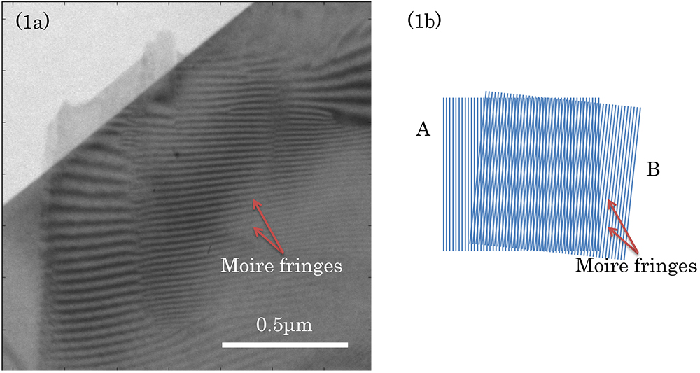
(1a) Bright-field image of mica showing Moiré fringes, taken at an accelerating voltage of 200 kV.
(1b) Schematic of rotation Moiré fringes. The fringes with an enlarged spacing appear when crystal lattices A and B which have the same spacing are superposed with a small orientation change.
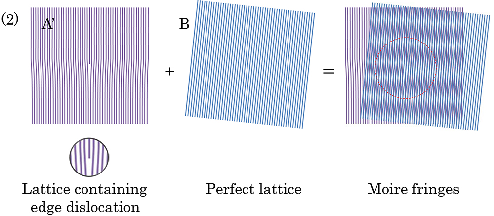
(2) Schematic of an enlarged dislocation image. An enlarged dislocation image is formed when a perfect lattice (B) is superposed on a lattice containing an edge dislocation (A’) with a small orientation change. It should be noted that the enlarged image is perpendicular to the original dislocation.
Related term
dislocation
150. Young fringe
When a beam exiting from a point source is passed through two slits, two waves exiting from the slits interfere with each other, resulting in formation of a fringe pattern. This fringe pattern is called "Young fringe(s)." As the distance between the two slits is smaller, the period of the Young fringes becomes larger. The Young fringe pattern is used to easily determine the resolution (information limit) of a TEM. In an actual experiment, two overlapping HREM images of an amorphous specimen are taken by shifting the electron beam within the exposure time to take one-frame CCD image, the images are acquired into a computer, and finally the diffraction pattern is obtained by FFT processing of the images. The Young fringes appear to be superposed on the diffraction pattern of the amorphous specimen. The information limit can be measured from the angular position (the radius of the Young fringe pattern) where the Young fringes disappear. The beam shift is chosen so that the Young fringes are easily seen with an appropriate separation.
(a) High-resolution TEM image of Au particles on a carbon thin film. (b) Fourier transform pattern of (a). (c) High-resolution TEM image taken by shifting the field of view using the deflector system. The relative shift and shift direction of the image are indicated by a yellow arrow. (d) Fourier transform pattern of (c). Fringes (Young fringes) corresponding to the relative shift are seen. The information limit can easily be measured from the angle at which the fringes disappear (indicated by a yellow circle).
Related term
optical diffraction method, information limit, FFT
151. Finite element method
"Finite element method (FEM)" is one of numerical analytical methods to obtain an approximate solution of partial differential equations that are difficult to solve analytically. First, an object of interest is divided into elements that each has a simple shape and a finite size. Next, physical quantities (temperature, stress, etc.) of each element are approximated by a simpler equation, and then the equations for the elements are combined to construct simultaneous equations. By solving the obtained simultaneous equation under the boundary conditions of the physical quantities at surfaces of the elements, the distribution of the physical quantities over the object are obtained. Since an object is subdivided to polyhedrons, FEM can be conveniently applied to complicated-shape objects. In electron microscopy, the method is used for calculation of mechanical strength and thermal distribution, calculation of distributions of magnetic fields and electrostatic fields of magnetic lenses and electrostatic lenses, etc. In the development of lens polepieces, aberration coefficients are obtained by calculation of electron trajectories using the magnetic field distributions obtained by FEM, and then the shapes of magnetic poles are optimized.
152. Laue function
The "Laue function" expresses the interference effect (diffraction intensity) of an electron (an X-ray and a neutron) due to a periodic arrangement of the unit cells in a crystal as a function of deviation from a Bragg angle. The angular width of diffraction depends on the number of the unit cells in the crystal when kinematical diffraction can be applied. As the number of unit cells in a crystal is greater, the diffraction peak becomes sharper. The Laue function tells us that the subsidiary maxima can be observed together with the Bragg peak (principal maximum) but they cannot usually be seen because the specimen normally used contains many unit cells. The Laue function cannot hold for a thick specimen to which dynamical diffraction must be applied. In this case, the angular width of diffraction depends on the magnitude of the crystal structure factor and strong subsidiary maxima appear.
Related term
kinematical diffraction, dynamical diffraction
153. Laue condition
A condition for a wave of an atomic scale wavelength, such as X-ray, electron and neutron, to cause diffraction by a crystal lattice. The "Laue condition" is equivalent to the Bragg condition. The Bragg condition is an instinctive scalar expression in the real space. On the other hand, the Laue condition is a vector expression in the reciprocal space, which is indispensable for advanced theoretical treatment of diffraction.
Related term
Bragg reflection, reciprocal lattice, reciprocal space
154. Laue zone
154-1. Laue zone
Laue zones are defined as the reciprocal lattice planes perpendicular to the direction of the incident beam. The Laue zone containing the origin (reciprocal lattice point corresponding to the incidence point) is called the zeroth-order Laue zone, and Laue zones of the n-th-order counted from the origin to the opposite direction of the incident beam are called the n-th-order Laue zones. The diffraction pattern is considered as the section of the reciprocal lattice points on the Laue zones cut by the Ewald sphere. The reciprocal lattice points belonging to the same Laue zone appear in a circular or an arc form in a diffraction pattern. The radius of the circle or arc is larger for higher-order Laue zones.
Related term
Ewald sphere, zeroth-order Laue zone (ZOLZ) reflection, higher-order Laue zone (HOLZ) reflection
154-2. higher-order Laue zone (HOLZ) reflection
"Laue zones" are defined as the reciprocal lattice planes perpendicular to the direction of the incident beam. A Laue zone containing the point of origin (reciprocal lattice point corresponding to the incidence point) is called the zeroth-order Laue zone (ZOLZ). The Laue zone of the n-th-order counted from the point of origin in the opposite direction of the incident beam is called the n-th-order Laue zone. Laue zones other than ZOLZ are termed "higher-order Laue zones (HOLZ)." The HOLZ reflections appear as narrow ring lines at positions distant from the center of a CBED pattern. The HOLZ reflections provide three-dimensional information on a crystal, whereas, the ZOLZ reflection gives only two-dimensional information on a crystal. The HOLZ reflections have larger diffraction vectors and their positions are sensitive to a slight change of the lattice parameters. Thus, these reflections are efficiently used for high-accuracy analysis of lattice distortions and crystal structures.
Related term
convergent-beam electron diffraction, CBED, Laue zone, zeroth-order Laue zone (ZOLZ) reflection
154-3. zeroth-order Laue zone (ZOLZ) reflection
"Laue zones" are defined as the reciprocal lattice planes perpendicular to the direction of the incident beam. A Laue zone containing the point of origin (reciprocal lattice point corresponding to the incidence point) is called the "zeroth-order Laue zone (ZOLZ)." The ZOLZ reflections appear around the transmitted beam in a CBED pattern, which have symmetry characteristic of a specimen crystal and show loose angular change. The ZOLZ reflections give two-dimensional information on a crystal projected along the direction of the incident beam.
Related term
convergent-beam electron diffraction,CBED, Laue zone, higher-order Laue zone (HOLZ) reflection
155. Rutherford scattering
"Rutherford scattering" is a phenomenon where a charged particle is scattered by Coulomb force of an atomic nucleus. The intensity of this scattering is proportional to the square of the atomic number Z and to (sinθ/2)-4, where θ expresses the scattering angle. In the case of the electron beam, the scattering approaches to Rutherford scattering at high-angles where scattering caused by the electron cloud around the atomic nucleus can be neglected.
156. Lichte focus
When a defocus amount is set at a value larger than Scherzer focus, a spatial frequency that leads the envelope function to 0 (zero) is increased. Then, the contrast transfer function starts to oscillate between positive and negative values at a lower spatial frequency than at Scherzer focus. In the case of reconstruction of an image by electron holography, the amplitudes with negative phase in the oscillation section can be added to the amplitudes with positive phase by converting the sign of the phase. In image reconstruction by holography, a structure image with a higher spatial resolution can be obtained by setting a defocus amount to a value twice or three times more than Scherzer focus. Such a defocus amount is named "Lichte focus" after the inventor of this technique.
Related term
Sherzer focus, electron holography
157. critical-voltage effect
"Critical voltage effect" means that the intensity of the second order reflection from a crystal lattice plane vanishes at a certain accelerating voltage of the incident electron beam when it is increased. The use of the effect enables us to refine (determine) the value of the crystal structure factor of the first order reflection with high accuracy.
158. excitation error
"Excitation error," expressed as sg, means a deviation from a Bragg condition for a certain reflection g. The excitation error is defined as the distance from the reciprocal lattice point g to a point on the Ewald sphere measured along the vertical direction to the upper surface of the specimen. When the Bragg condition is accurately satisfied, sg = 0. When the reciprocal lattice point is located outside the Ewald sphere, sg>0, whereas the reciprocal lattice point is located inside the Ewald sphere, sg<0. sg is an observable quantity with dimension of [length]-1. A dimensionless parameter (tilt parameter) "w = sg ・ξg," whereξg is the extinction distance, is used instead of sg as a useful parameter in the theoretical treatment. However, it should be noted that w is a non-observable quantity.
Related term
Bragg reflection, Ewald sphere, reciprocal lattice, dynamical diffraction
159. Lorentz electron microscopy
A method to observe magnetic domain structures of a ferromagnetic material using a TEM. Electrons passing through a ferromagnetic material undergo a Lorentz force that depends on the magnetization direction, thus their traveling direction changes (electrons are deflected). Adjoining magnetic domains experience different deflections, thus producing contrast between the magnetic domains. "Lorentz electron microscopy" has two modes: Fresnel mode and Foucault mode. In the Fresnel mode (defocus mode), the deflected electron-beams from the adjoining domains are superposed at the domain boundary, thus boundaries are observed as the light or dark line. In the Foucault mode (infocus mode), diffraction spots produced by the adjoining domains are displaced a little to each other on the back focal plane. When one of the two spots is selected for image formation, a bright image is obtained for the domain corresponding to the selected diffraction spot, whereas the dark image appears for the domain corresponding to the unselected diffraction spot. In an ordinary TEM, since the specimen is placed in a strong magnetic field, the entire specimen exhibits a single magnetic domain. To overcome this problem, a dedicated objective lens that applies nearly no magnetic field to the specimen position is used.
160. rocking curve
A "rocking curve" means the intensity distribution with the change of diffraction condition (with deviation from the Bragg angle). The rocking curve for a very thin specimen corresponds to the intensity distribution due to kinematical diffraction. That for a thick specimen corresponds to the intensity distribution due to dynamical diffraction and can be seen in a CBED pattern.
Related term
convergent-beam electron diffraction, CBED, kinematical diffraction, dynamical diffraction
161. Ronchigram
A Ronchigram is a projection image (pattern) of a specimen formed on the diffraction plane with a convergent incident electron beam focused near the specimen using a probe-forming lens. The Ronchigram enables us to determine the optical characteristics (amount of aberration) of the electron probe formed near the specimen using the probe-forming lens. The image is used to obtain the exact focus of the incident electron probe onto the specimen in STEM observations, to know the angular range of the electron probe with no aberration, and to compensate the axial astigmatism.
When the convergence point of the incident electron probe becomes closer to an amorphous specimen, the magnification of the specimen-shadow image (pattern) seen in the Ronchigram is increased. When the convergence point of the probe is exactly focused onto the specimen, the magnification of the Ronchigram or the shadow image becomes infinite and its intensity becomes uniform. By adjusting the Ronchigram to have a uniform intensity, the exact focus of the incident beam onto the specimen is confirmed. Measurement of the angular range of the area with a uniform intensity in the Ronchigram allows us to determine the angular range of the incident probe with no aberration or to know the quality of the electron-probe. If the third-order spherical aberration is not corrected, the area with a uniform electron intensity is confined to a small extent. When the aberration is corrected, the area is largely extended. This means that the angular range of the electron beam focused onto a point of the specimen is expanded due to vanishing of the aberration.
The Ronchigram obtained using a crystalline specimen exhibits interference fringes, when the incident beam with an incidence angle larger than the diffraction angle from a lattice plane of the crystal is illuminated onto the specimen with a small defocus. Appearance of the interference fringes means that the probe diameter on the focal plane is smaller than the lattice spacing. From this experiment, the probe size on the focal plane used for STEM observations can be known.
The term “Ronchigram” is named after V. Ronchi, who proposed the method to originally examine the performance of a lens of light optics.
Fig. (a) Ray diagram of Ronchigram. Fig. (b), Fig. (c) Ronchigram patterns obtained from an amorphous thin-film specimen. In the case of no aberration correction (Fig. (b)), the area with a uniform electron intensity is confined to a small extent (semi-angle: ~11 mrad). When the aberration is corrected (Fig. (c)), the area is largely extended (semi-angle: ~45 mrad).
Related term
optical diffraction method
162. Larmor rotation
When magnetic-field components vertical to a velocity component of an electron exist, the electron undergoes a rotary motion vertical to the the magnetic-field components. This rotary motion is called “Larmor rotation.” In a transmission electron microscope (TEM), when an electron transmitted through a specimen travels in the vertical direction (from above to below), the electron undergoes Lamor rotation due to the horizontal magnetic-field components of the magnetic-field lenses. Since the imaging system uses multi-stage magnetic-field lenses, the enlarged image of a specimen is formed onto the fluorescent screen with a certain rotation against the specimen. The rotation angle is determined by the accelerating voltage of the electron and the total ampere turns of the magnetic-field lenses.
Related term
lens action in the magnetic field
163. lens action in the magnetic field
When an electron passes through the magnetic field produced by the polepiece of a lens in the vertical direction (from above to below), the electron traveling at an off-axis position firstly undergoes Lamor rotation due to the horizontal components of the magnetic field. Then, the electron receives a converging force toward the optical axis due to a Lorentz force between the rotational velocity component of the electron and the vertical component of the magnetic field of the lens. The magnetic-field components, which yield the converging force proportional to (angle between the electron beam and the optical axis), are used as the lens action. The strength of the lens action is controlled by the electric current applied to the coils producing the electro-magnetic-field.
Related term
Larmor rotation
164. differential phase contrast imaging
Differential phase contrast imaging is a STEM method to visualize an electromagnetic field in a specimen by measuring the deflection of an electron beam due to the field at each beam-scan point. The beam deflection is measured with a segmented detector or a pixelated detector. When a segmented detector composed of four segments is used (see Figure below), the angle and the direction of the beam deflection (beam shift on the detector plane) are measured from the difference between the signal amounts acquired with the two segments opposed to each other. It is noted that the naming “differential phase contrast” of this imaging method is originated from that the deflection of the electron beam causes the differential or gradient of the phase of the electron wave. Differential phase contrast imaging is utilized for observations of micrometer to nanometer scale magnetic domains. In recent years, this imaging method has been applied to analysis of electric fields, and the electric field at the atomic scale has been observed using a transmission electron microscope equipped with a Cs corrector.
Fig.(a) Schematic of detection of the electron beam deflection in a specimen using a segmented detector (In case that the electron beam is not deflected by the specimen). Fig.(b) A STEM detector in this case is composed of four segments. The shadow of the condenser aperture is projected onto the detector.Top view of the detector and the electron beam seen along the incident beam direction. The signal amounts are the same for the four segments. Thus, there is no difference between the signal amounts acquired from the two segments opposed to each other.
Fig.(c) Schematic of detection of the electron beam deflection in a specimen using a segmented detector (In case that the electron beam is deflected by a specimen). Fig.(d) Top view of the detector and the electron beam seen along the incident beam direction. When the beam is deflected in the positive direction of the x axis, the signal amounts obtained by subtracting Idet3 from Idet1 becomes a negative value, whereas there is no difference between the signal amounts Ide2 and Idet4. As a result, the beam is found to be deflected in the positive direction of the x axis, and the deflection angle is measured from the absolute value of the signal difference.
165. Line synchronization
"Line synchronization" means a synchronization of the timing to start electron-beam scan in each horizontal direction with the phase of the AC power wave when acquiring a STEM image. When the line synchronization function is operated at the image acquisition, the influence of external disturbance with the frequency (or the multiples of the frequency) of the AC power-source becomes same on every scan line, and then the external disturbance happening in each scan line apparently disappears. As a result, the fine noise in the horizontal scan line disappears, and the influence of the external disturbance is reduced from the STEM image.
166. Dwell time
"Dwell time" means a time for an electron beam to stay per pixel at acquisition of a STEM image by electron-beam scan. The Dwell time is an index for the scan speed of the electron beam. When the Dwell time is multiplied by the number of scan pixels in one horizontal line scan, and then the Flyback time is added, the scan time for one horizontal line scan is obtained. When this scan time is multiplied by the number of the vertical scans (horizontal scan lines), the acquisition time of one scanning image is calculated.
167. Flyback time
"Flyback time" means the standby time for a scanning electron beam from the end of a horizontal scan to the start of the next scan at swing-back of the electron beam when acquiring a STEM image. The electronic circuit responds non-linearly at the beginning of each horizontal line scan, giving rise to the distortion of the scanning waveform in a certain time zone. Only the linear response time zone of the electronic circuit should be used to eliminate distortions of the STEM image. Thus, the Flyback time is set longer than the non-linear response time zone, removing the response time zone with the distorted waveform from the image acquisition. As a result, the STEM image is obtained without distortion.
168. ptychography
Ptychography is a method to reconstruct the crystal structure (image) of a specimen from the diffraction patterns obtained from each point (area) scanned over a specimen using a convergent probe so that a part of the illuminated area overlaps. “Ptycho” means “fold” in Greek. This method has been used in X-ray crystal structural analysis. Ptychography for Electron Microscopy has attracted attention as one of the method to obtain the structural image (phase recovery) of atomic resolution since about 2012, owing to the advent of a high-speed and high-sensitivity camera that achieves fast acquisition of a two-dimensional (2D) digital image, together with improvement of microscope stability and advancement of the aberration corrector. In particular, it has been reported in recent electron ptychography studies that low-noise and high-contrast structure images are obtained, thus gaining increased attention. In transmission electron microscopy, the following two types of ptycography methods are being conducted.
1) Method to scan a specimen with a defocused convergent electron probe (Fig. (a)) A specimen is illuminated with a defocused convergent electron probe to broaden the illumination area. The probe is scanned on the specimen so that the adjacent illumination areas are partially overlapped to each other. The scan points of the probe are normally a few 10 points × a few 10 points or less depending on the scanning area and probe size. The procedure to obtain a structure image (phase image) by means of this type of ptychography is as follows: The initial specimen function is assumed equal to 1 and the probe function is assumed to be a box function. The specimen exit-wave function (a product of the specimen and probe functions) is Fourier-transformed to obtain a diffraction pattern, the intensities of which are replaced by those of the pattern acquired experimentally. The updated diffraction pattern is then transformed back to an image in the real space by an inverse Fourier transform, which gives a new revised exit-wave function for this probe position. The probe function obtained is replaced with the correct function or the original one. And the above procedure is repeated. Then, the calculation moves to the next position. Aforementioned procedure is repeated until the difference of the calculated and experimental diffraction patterns becomes sufficiently small. The resultant structural image (phase image) of the specimen is shown in Fig. (c). The present method is similar to conventional incoherent diffractive imaging. It should be however noted that non-unique solution problem arising in diffractive imaging is overcome due to the additional constraint, in which the specimen function in the overlapping region of the adjacent illumination areas have to be the same in the calculation for the diffraction patterns recorded. Furthermore, the issue of a limited field of view is cleared by scanning technique. 2) Method to scan a specimen with a focused convergent electron probe (Fig. (b)) A specimen is illuminated with a focused convergent electron probe.The convergent beam electron diffraction (CBED) pattern is recorded as a 2D image. The probe is scanned two dimensionally on the specimen. Scan points of the probe becomes a huge four-dimensional (4D) data set (2D CBED patterns +2D scan points), normally exceeding a few 10 thousands points. The procedure for reconstructing a high-contrast structure image is as follows. First, the 4D data set RK (2D scan points R + 2D CBED patterns K) is Fourier-transformed with respect to the 2D scan points R to obtain another 4D data set QK (2D spatial frequencies Q + 2D CBED patterns K). In the overlapping area (K’) of the transmitted disc and a neighboring diffracted disc of the CBED pattern for a certain 2D spatial frequency q, the intensity of the Fourier component q of the structure appears (bottom of Fig. (b)). To improve the signal-to-noise ratio of the structure image (phase image) to be obtained, the intensities outside the interference area (K’) are set to be 0 (zero). And the sign (phase) of the intensities in the interference area (K) located symmetrically with respect to the transmitted disc is reversed. By this processing, the intensities of the two areas (K’ and K), which are normally canceled out when integrating, can be added positively or enhanced. Then, the intensities of the two areas (K’ and K) of the 2D CBED pattern (bottom of Fig. (b)) are integrated for each spatial frequency component q of the 4D data set QK, so that a 2D spatial frequency pattern Q' is created. Finally, this 2D spatial frequency pattern Q' is inverse-Fourier transformed to obtain the structure image (phase image) of the specimen (Fig. (d)). (Proofread by Dr. Peng Wang, Nanjing University)
Fig. 1 (a) Ptychography in which a specimen is scanned with a defocused convergent electron probe so that adjacent illumination areas are partially overlapped to each other. The illumination area is about a few nm to a few 10 nm in diameter. The number of the scan points is normally a few 10 times a few 10 or less. (b) Ptychography in which a specimen is scanned with a focused convergent electron probe (probe diameter: about 0.3 nm or less). The number of the scan points is a few 100 times a few 100 (the total number exceeding a few 10 thousands) like the case of ordinary STEM. A high-speed and high-sensitivity camera (pixelated STEM detector) is used to obtain a series of the CBED patterns. (c) Structure image (Phase image) of a mono-layer of MoS2 reconstructed by the defocus method (a). (Data courtesy: Dr. Peng Wang, Nanjing University) (d) Structure image (Phase image) of a mono-layer graphene reconstructed by the focus method (b).
Fig. 2 Comparison of a reconstructed structure image (phase) obtained by Ptychography in which a specimen is scanned with a convergent probe and a simultaneously-obtained ABF image of a mono-layer graphene acquired at an accelerating voltage of 200 kV. (a) Structure image (phase) of graphene reconstructed from 4D data set. Here, the atomic sites appear bright. (b) Ordinal ADF image simultaneously acquired with the 4D data set. Comparison of the two images elucidates that the reconstructed structure image (phase) has a higher signal-to-noise ratio and provides higher contrast than those of the ADF image.
169. autoradiography
Autoradiography in Electron Microscopy is a method to observe a specific site of a biological specimen labeled with a substance containing a radioactive isotope. The method is implemented in the following procedure. A substance containing a radioactive isotope is doped into a biological specimen for labeling specific tissues or cells. The biological specimen is thinned down to an ultrathin section and a photo-sensitive emulsion (silver halide suspension) is applied to the thin section. Silver halides in the vicinity of the labeled sites are exposed with β rays emitted from the radioactive isotope. When photo-developed, silver particles are segregated at the labeled sites. When the section is observed with a transmission electron microscope, the positions of the labeled tissues or cells can be identified from the localized silver particles. In order to perform high-resolution observation of the sites of the labeled tissues or cells, tritium (which emits small energy β-rays) is often used as a radioactive isotope because tritium causes small silver segregates in the photosensitive emulsion. An example of Autoradiography in Electron Microscopy: Thymidine containing radioactive tritium is applied to label the sites where cell divisions are active in a biological specimen. The labeled sites are revealed from the segregated silver particles by observing the electron microscope image of the specimen.
170. reliability factor (R-factor)
In structure analysis using an X-ray beam or an electron beam, Reliability factor (R-factor) is an index that expresses the degree of reliability for the structure obtained from an experimental structure analysis result. When the crystal structure factor obtained from an experimental diffraction pattern is expressed as Fobs (hkl), and the crystal structure factor calculated from the assumed structure model is expressed as Fcal (hkl), the R-factor is defined by the following equation.

Here, (hkl) is an index of Bragg reflection (Mirror index) and the sum of the right side of the equation is taken for all of the experimentally measured reflections. In the structure analysis, so as to minimize the R-factor, the parameters (symmetry, lattice constant, atomic coordinate, etc.) of the crystal structure (structure model) are determined. When the experimentally-obtained crystal structure factor coincides fully with the crystal structure factor calculated from the determined structure, the R-factor becomes 0 (zero). When the crystal structure which provides the highest reproducibility of the experimental value is obtained, the value of the R-factor is about 0.05 for X-ray crystallography and is about 0.2 for electron crystallography.
